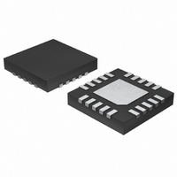
MAX1543ETP+T Maxim Integrated Products, MAX1543ETP+T Datasheet - Page 10

MAX1543ETP+T
Manufacturer Part Number
MAX1543ETP+T
Description
IC DC-DC CONV TFT-LCD 20-TQFN
Manufacturer
Maxim Integrated Products
Datasheet
1.MAX1543ETP.pdf
(20 pages)
Specifications of MAX1543ETP+T
Applications
Controller, TFT, LCD
Voltage - Input
2.6 ~ 5.5 V
Number Of Outputs
2
Voltage - Output
2.6 ~ 13 V
Operating Temperature
-40°C ~ 85°C
Mounting Type
Surface Mount
Package / Case
20-TQFN Exposed Pad
Lead Free Status / RoHS Status
Lead free / RoHS Compliant
The MAX1542 typical application circuit (Figure 1) and
the MAX1543 typical application circuit (Figure 2) gen-
erate an +8V source driver supply and approximately
+22V and -7V gate driver supplies for TFT displays. The
input voltage is from +2.6V to +5.5V. Table 1 lists rec-
ommended components and Table 2 lists contact infor-
mation for component suppliers.
The MAX1542/MAX1543 include a high-performance
step-up regulator, two high-current operational ampli-
fiers, and startup timing and level-shifting functionality
useful for active matrix TFT LCDs. Figure 3 shows the
MAX1542/MAX1543 functional diagram.
TFT LCD DC-to-DC Converter with
Operational Amplifiers
10
MAX1542
______________________________________________________________________________________
14
16
17
18
19
—
—
PIN
Typical Application Circuits
MAX1543
14
15
16
17
18
19
20
Detailed Description
NAME
COMP
FREQ
DRN
DEL
CTL
FB
IN
Supply Voltage. IN can range from 2.6V to 5.5V.
Oscillator Frequency Select Input. Pull FREQ low or leave it unconnected for 640kHz
operation. Connect FREQ high for 1.2MHz operation. This input has a 5µA pulldown
current.
Step-Up Converter Feedback Input. Regulates to 1.24V (nominal). Connect a resistor-
divider from the output (V
within 5mm of FB.
Step-Up Regulator Error Amplifier Compensation Point. Connect a series RC from COMP
to AGND. See the Loop Compensation section for component selection guidelines.
High-Voltage Switch Delay Input. Connect a capacitor from DEL to AGND to set the high-
voltage switch startup delay. A 5µA current source charges C
For the MAX1542, the high-voltage switch between SRC and COM is disabled until V
exceeds 1.24V. Following the delay period, CTL controls the state of the high-voltage
switch.
For the MAX1543, the switches between SRC, COM, and DRN are disabled and a 1kΩ
pulldown between COM and PGND is enabled until V
delay period, the 1kΩ pulldown is released and CTL controls the state of the high-voltage
switches (see the Delay Control Circuit section).
High-Voltage Switch Control Input. When CTL is high, the high-voltage switch between
COM and SRC is on and the high-voltage switches between COM and DRN (MAX1543)
are off. When CTL is low, the high-voltage switch between COM and SRC is off and the
high-voltage switches between COM and DRN (MAX1543) are on. CTL is inhibited by the
undervoltage lockout and when V
Switch Input. Drain of the internal high-voltage back-to-back P-channel MOSFETs
connected to COM.
MAIN
The MAX1542/MAX1543 main step-up converter
switches at 1.2MHz or 640kHz (MAX1543 only) (see the
Oscillator Frequency (FREQ) section). The devices
employ a current-mode, fixed-frequency, pulse-width
modulation (PWM) architecture to maximize loop band-
width providing fast transient response to pulsed loads
found in source drivers for TFT LCD panels. The high-
switching frequency also allows the use of low-profile
inductors and capacitors to minimize the thickness of
LCD panel designs. The integrated high-efficiency
MOSFET and the IC’s built-in digital soft-start function
reduce the number of external components required
while controlling inrush current. The output voltage of
the main step-up converter (V
to 13V with an external resistive voltage-divider at FB.
) to FB to analog ground (AGND). Place the resistor-divider
DEL
is less than 1.24V.
FUNCTION
Pin Description (continued)
DEL
Main Step-Up Converter
exceeds 1.24V. Following the
DEL
MAIN
.
) can be set from V
DEL
IN


