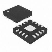
MAX8723ETE+T Maxim Integrated Products, MAX8723ETE+T Datasheet - Page 8

MAX8723ETE+T
Manufacturer Part Number
MAX8723ETE+T
Description
IC REG FOR LCD DISPLAY 16-TQFN
Manufacturer
Maxim Integrated Products
Specifications of MAX8723ETE+T
Applications
Converter, LCD
Voltage - Input
6 ~ 13.2 V
Number Of Outputs
1
Voltage - Output
3.3V, 2 ~ 3.6 V
Operating Temperature
-40°C ~ 85°C
Mounting Type
Surface Mount
Package / Case
16-TQFN Exposed Pad
Lead Free Status / RoHS Status
Lead free / RoHS Compliant
Low-Cost, Internal-Switch, Step-Down
Regulator for LCD Displays
8
PIN
EP
10
11
12
13
14
15
16
_______________________________________________________________________________________
1
2
3
4
5
6
7
8
9
NAME
PGND
SHDN
VCC2
FSEL
GND
OUT
VCC
BST
REF
EXT
I.C.
INL
FB
EP
LX
VL
IN
Step-Down Regulator Input Voltage (6V to 13.2V). Bypass IN to PGND with a minimum 4.7µF ceramic
capacitor close to the IC.
Step-Down Regulator Inductor Connection. Internally connected to the junction of the internal high-side and
low-side MOSFETs.
Step-Down Regulator Bootstrap Capacitor Connection for High-Side Gate Driver. Connect a 0.1µF ceramic
capacitor from BST to LX.
Internal Connection. Make no connection to this pin.
Output Voltage-Sense Input and the Negative Input to the Current-Sense Amplifier. Connect OUT to the step-
down regulator output.
Step-Down Converter Feedback Input:
1)
2)
Step-Down Regulator Power Ground
External Synchronous Rectifier Gate Driver Output. To use a synchronous rectifier (optional), connect EXT to
the gate of the external MOSFET. EXT is low in shutdown.
Internal 5V Linear Regulator Supply Input. Bypass INL to GND with a 0.22µF ceramic capacitor close to the IC.
5V Internal Linear Regulator Output. Bypass VL to GND with a 1µF minimum ceramic capacitor. VL is enabled
in shutdown and during faults. See the Linear Regulator (VL) section for further information.
Internal Reference Supply Input. Connect VCC to VL.
Analog Ground
Reference Output. Bypass REF to GND with 0.22µF ceramic capacitor.
Switching Frequency Selection Input. This tri-level logic input sets the SMPS’s switching frequency:
Shutdown Control Input. When SHDN is low, the step-down regulator power output is disabled, but REF and
VL remain on.
Connect VCC to VL.
Exposed Backside Pad. For better thermal management, this pad should be soldered to an analog ground
plane connected to sufficient copper through multiple vias.
FSEL = GND, f
FSEL = VCC, f
FSEL = REF, f
Connect FB to GND for a fixed 3.3V output.
Connect FB to the center tap of a resistive voltage-divider between the step-down regulator output and
GND for an adjustable output from 2.0V to 3.6V.
SW
SW
SW
= 500kHz
= 1.0MHz
= 1.5MHz
FUNCTION
Pin Description


