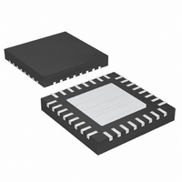
MAX1997ETJ+T Maxim Integrated Products, MAX1997ETJ+T Datasheet - Page 28

MAX1997ETJ+T
Manufacturer Part Number
MAX1997ETJ+T
Description
IC PWR SUPPLY TFT LCD 32TQFN
Manufacturer
Maxim Integrated Products
Datasheet
1.MAX1997ETJ.pdf
(31 pages)
Specifications of MAX1997ETJ+T
Applications
Controller, TFT, LCD
Voltage - Input
2.7 ~ 5.5 V
Number Of Outputs
5
Voltage - Output
2.7 ~ 13 V
Operating Temperature
0°C ~ 85°C
Mounting Type
Surface Mount
Package / Case
32-TQFN Exposed Pad
Lead Free Status / RoHS Status
Lead free / RoHS Compliant
Quintuple/Triple-Output TFT LCD Power Supplies
with Fault Protection and VCOM Buffer
Figure 12. High-Current Loops of Step-Up Regulator
Figure 13. Operation with Output Voltage >13V Using
Cascoded MOSFET
28
Figure 11. Optimizing VCOM Buffer Drive Current
V
C
IN
______________________________________________________________________________________
IN
V
V
GAMMA
IN
V
N
REGULATOR
VCOM BUFFER
STEP-UP
L
MAX1997
MAX1998
GROUND IMPEDANCE
0.47µF
LX
FB
PGND
R
B
C
B
D
TO TFT LCD
BACKPLANE
V
P
V
15V
MAIN
V
C
OUT
OUT
6) To ensure stability, choose CLDO large enough so
A capacitor connected between the regulator output and
the feedback node can improve the transient response
and reduce the noise coupled into the feedback loop
(Figure 1).
If a low-dropout solution is needed, an external P-channel
MOS pass transistor can be used for REG 1. However, a
PMOS-based linear regulator requires higher output
capacitance to stabilize the loop. The high gate capaci-
tance of the P-channel MOSFET lowers f
can cause instability. A large output capacitor must be
used to reduce the unity-gain bandwidth and ensure that
the pole is well above the unity-gain crossover frequency.
A ceramic capacitor of at least 30µF is recommended for
V
Connect the inverting input FBNB directly to the output
OUTB to configure the buffer as a voltage follower.
Adjust the buffer’s output voltage by connecting a volt-
age-divider from the gamma reference V
GND with the center tap connected to the noninverting
input FBPB (Figure 1). Select R14 in the 10kΩ to 100kΩ
range. Calculate R13 with the following equation:
The VCOM buffer is designed to be stable with a
0.47µF capacitor from OUTB to GND. The charge and
discharge currents of the VCOM buffer output can be
optimized by adding resistor R
backplane load and a ceramic capacitor C
larger) in parallel with the backplane load (Figure 11).
Start with a 10Ω resistor, then gradually increase the
value of R
buffer power dissipation. Increasing the value of C
improves the efficiency of the VCOM buffer.
IN
that the crossover occurs well before the poles and
zero calculated in steps 2 to 5. The poles in steps 3
and 4 generally occur at several megahertz and
using ceramic capacitors ensures the ESR zero
occurs at several megahertz as well. Placing the
crossover below 500kHz is sufficient to avoid the
amplifier-delay pole and generally works well,
unless unusual component choices or extra capaci-
tances move the other poles or zero below 1MHz.
= 2.7V, V
B
, balancing between display quality and
OUT
R13 = R14
= 2.5V, and I
V
GAMMA
V
FBPB
LOAD
B
in series with the LCD
= 250mA.
−
1
VCOM Buffer
POLE(CIN)
GAMMA
B
(1µF or
and
to
B


