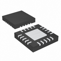
MAX1515ETG+T Maxim Integrated Products, MAX1515ETG+T Datasheet - Page 2

MAX1515ETG+T
Manufacturer Part Number
MAX1515ETG+T
Description
IC REG DDR LV 24-TQFN
Manufacturer
Maxim Integrated Products
Datasheet
1.MAX1515ETG.pdf
(24 pages)
Specifications of MAX1515ETG+T
Applications
Converter, DDR
Voltage - Input
1.3 ~ 3.6 V
Number Of Outputs
2
Voltage - Output
0.5 ~ 2.7 V
Operating Temperature
-40°C ~ 85°C
Mounting Type
Surface Mount
Package / Case
24-TQFN Exposed Pad
Lead Free Status / RoHS Status
Lead free / RoHS Compliant
ABSOLUTE MAXIMUM RATINGS
V
MODE, IC to GND ....................................................-0.3V to +4V
COMP, FB, REF, REFIN, REFOUT, PGOOD
FBSEL0, FBSEL1, TOFF, SKIP, SS to GND....-0.3V to (V
V
IN to V
PGND to GND ...................................................... -0.3V to +0.3V
LX to BST................................................................. -4V to +0.3V
BST to GND .......................................................... -0.3V to +8.0V
Low-Voltage, Internal Switch,
Step-Down/DDR Regulator
Note 1: LX has clamp diodes to PGND and IN. If continuous current is applied through these diodes, thermal limits must be observed.
Stresses beyond those listed under “Absolute Maximum Ratings” may cause permanent damage to the device. These are stress ratings only, and functional
operation of the device at these or any other conditions beyond those indicated in the operational sections of the specifications is not implied. Exposure to
absolute maximum rating conditions for extended periods may affect device reliability.
ELECTRICAL CHARACTERISTICS
(Circuit of Figure 1, V
erwise noted. Typical values are at T
2
PWM CONTROLLER
Input Voltage Range
Output Adjust Range
Feedback Voltage Accuracy
Feedback Load-Regulation Error
CC
DD
to GND.........................................................-0.3V to (V
, V
_______________________________________________________________________________________
to V
DD
DD
CC
, LX, SHDN to GND ...................................-0.3V to +4V
....................................................-0.3V to (V
PARAMETER
...........................................................-0.3V to + 0.3V
IN
= +3.3V, V
CC
A
SYMBOL
V
= V
= +25°C.)
CC
V
V
REFIN
V
V
FB
DD
, V
FB
IN
-
DD
=
SHDN = MODE = +3.3V, V
V
V
MODE = V
V
I
MODE = low
V
SKIP = V
LOAD
OUT
IN
IN
IN
DD
CC
CC
= +1.3V to +3.6V, I
= +3.3V, I
= +3.3V,
≤ V
+ 0.3V)
+ 0.3V)
+ 0.3V)
= 0,
CC
IN
CC
LOAD
FBSEL0 = V
FBSEL1 = V
REFIN = REF
FBSEL0 = V
FBSEL1 = GND,
REFIN = REF
FBSEL0=GND
FBSEL1=V
REFIN=REF
FBSEL0=GND
FBSEL1=GND
REFIN=0.5V
CONDITIONS
= 0,
LX Current (Note 1).............................................................±4.7A
REF Short Circuit to GND ...........................................Continuous
REFOUT Short Circuit to GND....................................Continuous
Continuous Power Dissipation (T
Operating Temperature Range ...........................-40°C to +85°C
Junction Temperature ......................................................+150°C
Storage Temperature Range .............................-65°C to +150°C
Lead Temperature (soldering, 10s) .................................+300°C
24-Pin Thin QFN (derate 20.8mW/°C above +70°C;
part mounted on 1in
LOAD
REFIN
CC
CC
CC
CC
= 0 to 3A,
,
,
,
= V
T
to +85°C
T
+85°C
T
to +85°C
T
+85°C
T
to +85°C
T
+85°C
T
to +85°C
T
+85°C
T
to +85°C
T
+85°C
A
A
A
A
A
A
A
A
A
A
REF
= +25°C
= 0°C to
= +25°C
= 0°C to
= +25°C
= 0°C to
= +25°C
= 0°C to
= +25°C
= 0°C to
, SKIP = GND, T
2
of 1oz copper)........................1667mW
2.463
2.450
1.782
1.773
1.477
1.470
0.492
0.490
MIN
1.3
3.0
0.5
-3
-4
A
= +70°C)
A
= 0°C to +85°C, unless oth-
1.800
1.800
1.500
1.500
0.500
0.500
TYP
2.5
2.5
0.1
0
0
2.537
2.550
1.827
1.836
1.523
1.530
0.508
0.510
MAX
3.6
3.6
2.7
+3
+4
UNITS
mV
%
V
V
V


