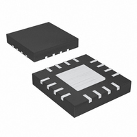
MAX1889ETE+ Maxim Integrated Products, MAX1889ETE+ Datasheet - Page 2

MAX1889ETE+
Manufacturer Part Number
MAX1889ETE+
Description
IC PWR SUP TRPL LCD 16-TQFN
Manufacturer
Maxim Integrated Products
Datasheet
1.MAX1889ETET.pdf
(32 pages)
Specifications of MAX1889ETE+
Applications
Controller, TFT, LCD
Voltage - Input
2.7 ~ 5.5 V
Number Of Outputs
3
Voltage - Output
2.7 ~ 13 V
Operating Temperature
0°C ~ 85°C
Mounting Type
Surface Mount
Package / Case
16-TQFN Exposed Pad
Lead Free Status / RoHS Status
Lead free / RoHS Compliant
ABSOLUTE MAXIMUM RATINGS
IN, SHDN, OCN, OCP,
PGND to GND.....................................................................±0.3V
LX to PGND ............................................................-0.3V to +14V
DRVP to GND .........................................................-0.3V to +30V
REF, GATE, TGND to GND ..........................-0.3V to (V
DRVN to GND .....................................(V
Triple-Output TFT LCD Power Supply
with Fault Protection
ELECTRICAL CHARACTERISTICS
(V
Stresses beyond those listed under “Absolute Maximum Ratings” may cause permanent damage to the device. These are stress ratings only, and functional
operation of the device at these or any other conditions beyond those indicated in the operational sections of the specifications is not implied. Exposure to
absolute maximum rating conditions for extended periods may affect device reliability.
2
IN Supply Range
IN Undervoltage Lockout
(UVLO) Threshold
IN Quiescent Current
IN Shutdown Current
REF Output Voltage
Thermal Shutdown
MAIN STEP-UP REGULATOR
Main Output Voltage Range
Operating Frequency
Oscillator Maximum Duty Cycle
FB Regulation Voltage
FB Fault Trip Level
Load Regulation
Line Regulation
FB Input Bias Current
LX Switch On-Resistance
LX Leakage Current
LX Current Limit
LX RMS Current Rating
Soft-Start Period
Soft-Start Step Size
POSITIVE LINEAR-REGULATOR CONTROLLER
FBP Regulation Voltage
FBP Fault Trip Level
FBP Input Bias Current
FBP Effective Transconductance
IN
FB, FBP, FBN, FREQ to GND ...............................-0.3V to +6V
_______________________________________________________________________________________
= 3V,
SHDN = IN, C
PARAMETER
REF
= 0.22µF, PGND = GND, T
SYMBOL
R
V
V
V
LX(ON)
V
f
I
IN
I
UVLO
V
V
MAIN
OSC
I
I
t
FBP
I
LIM
REF
FBP
FB
LX
SS
IN
FB
IN
- 28V) to (V
350mV typical
hysteresis
V
V
-2µA < I
V
V
I
V
I
V
V
V
Not tested
I
V
V
V
LX
MAIN
DRVP
FB
FREQ
FREQ
FB
IN
FB
LX
FBP
FBP
DRVP
SHDN
A
= 200mA, slope = 0 (Note 2)
= 0°C to +85°C. Typical values are at T
= 2.7V to 5.5V
IN
IN
= 13V
= V
falling
= 1.5V
falling
= 1.25V
= 0 to full load
= 0.2mA
+ 0.3V)
+ 0.3V)
= V
= 0V
= 10V, I
= 0, V
FBP
REF
IN
= 1.5V, V
< 50µA
IN
DRVP
CONDITIONS
= 5V
Continuous Power Dissipation (T
Operating Temperature Range
Junction Temperature ......................................................+150°C
Storage Temperature Range .............................-65°C to +150°C
Lead Temperature (soldering, 10s) .................................+300°C
= 0.1mA to 2mA
FBN
16-Pin QFN (derate 19.2mW/°C above +70°C) .........1538mW
MAX1889EGE ..................................................-40°C to +85°C
V
V
IN
IN
= 0V (Note 1)
rising
falling
A
= +25°C, unless otherwise noted.)
1.231
1.229
1.213
2.55
0.85
0.95
-100
0.96
MIN
V
-50
2.7
2.2
1.6
80
75
IN
A
= +70°C)
V
4096 /
REF
1.250
1.242
f
TYP
2.35
0.01
1.25
160
500
-1.6
250
OSC
2.7
0.1
1.0
0.2
2.1
1.0
85
1
/32
1.269
1.254
1.288
MAX
+100
2.85
1.15
1.05
1.04
+50
450
5.5
2.5
1.0
1.0
2.8
1.4
13
90
20
UNITS
MHz
kHz
%/V
mΩ
mA
mS
µA
°C
nA
µA
nA
%
%
V
V
V
V
V
V
A
A
s
V
V
V


