FAN5059M Fairchild Semiconductor, FAN5059M Datasheet - Page 2
FAN5059M
Manufacturer Part Number
FAN5059M
Description
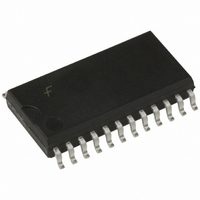
IC CTRLR DC/DC PROG SYNC 24SOIC
Manufacturer
Fairchild Semiconductor
Datasheet
1.FAN5059MX.pdf
(18 pages)
Specifications of FAN5059M
Applications
Controller, VRM8.5
Voltage - Input
5V
Number Of Outputs
1
Voltage - Output
1.3 ~ 3.5 V
Operating Temperature
0°C ~ 70°C
Mounting Type
Surface Mount
Package / Case
24-SOIC (7.5mm Width)
Output Voltage
2 V
Output Current
18 A
Input Voltage
5 V
Switching Frequency
300 KHz
Operating Temperature Range
0 C to + 70 C
Mounting Style
SMD/SMT
Duty Cycle (max)
85 %
Lead Free Status / RoHS Status
Lead free / RoHS Compliant
Other names
FAN5059M_NL
FAN5059M_NL
FAN5059M_NL
Available stocks
Company
Part Number
Manufacturer
Quantity
Price
Company:

Part Number:
FAN5059M
Manufacturer:
Fairchild Semiconductor
Quantity:
135
Part Number:
FAN5059M
Manufacturer:
FAIRCHILD/ن»™ç«¥
Quantity:
20 000
Company:
Part Number:
FAN5059MX
Manufacturer:
MITEL
Quantity:
500
Part Number:
FAN5059MX
Manufacturer:
FAIRCHILD/ن»™ç«¥
Quantity:
20 000


Pin Definitions
FAN5059
currents in excess of 16A from a 5V source with minimal
external circuitry. Synchronous-mode operation offers opti-
mum efficiency over the entire specified output voltage range.
An on-board precision low TC reference achieves tight toler-
ance voltage regulation without expensive external compo-
nents, while Programmable Active Droop
tailoring of voltage for the most demanding load transients. The
FAN5059 includes linear regulator controllers for Vtt termina-
tion (1.5V), Vclock (2.5V), and Vnorthbridge (1.8V) or Vagp
(selectable 1.5V/3.3V), each adjustable with an external divider.
The FAN5059 also offers integrated functions including Power
Good, Output Enable/Soft Start and current limiting, and is
available in a 24 pin SOIC package.
2
Number Pin Name
Pin
4-8
10
11
12
13
14
15
16
17
18
19
20
21
22
23
24
1
2
3
9
HIDRV
SW
GNDA
VID0-4
VTTGATE
VTTFB
VCKGATE
VCKFB
VAGPFB
VAGPGATE
TYPEDET
ENABLE/SS Output Enable. A logic LOW on this pin will disable all outputs. An internal current source
PWRGD
ILIM
DROOP
VFB
VCCA
GNDP
LODRV
VCCP
Pin Function Description
High Side FET Driver. Connect this pin through a resistor to the gate of an N-channel
MOSFET. The trace from this pin to the MOSFET gate should be <0.5".
High side Driver Source and Low side Driver Drain Switching Node. Together with
DROOP and ILIM pins allows FET sensing for Vcc current.
Analog Ground. Return path for low power analog circuitry. This pin should be
connected to a low impedance system ground plane to minimize ground loops.
Voltage Identification Code Inputs. These open collector/TTL compatible inputs will
program the output voltage over the ranges specified in Table 2. Pull-up resistors are
internal to the controller.
Gate Driver for VTT Transistor. For 1.5V output.
Voltage Feedback for VTT.
Gate Driver for VCK Transistor. For 2.5V output.
Voltage Feedback for VCK.
Voltage Feedback for VAGP.
Gate Driver for VAGP Transistor. For 3.3/1.5V output.
Type Detect. Sets 3.3V or 1.5V for AGP.
allows for open collector control. This pin also doubles as soft start for all outputs.
Power Good Flag. An open collector output that will be logic LOW if any output voltage
is more than ±12% outside of the nominal output voltage setpoint.
Vcc Current Feedback. Pin 18 is used in conjunction with pin 2 as the input for the Vcc
current feedback control loop. Layout of these traces is critical to system performance.
See Application Information for details.
Droop set. Use this pin to set magnitude of active droop.
Vcc Voltage Feedback. Pin 20 is used as the input for the Vcc voltage feedback control
loop. See Application Information for details regarding correct layout.
Analog VCC. Connect to system 5V supply and decouple with a 0.1µF ceramic capacitor.
Power Ground. Return pin for high currents flowing in pin 24 (VCCP).
Vcc Low Side FET Driver. Connect this pin through a resistor to the gate of an N-channel
MOSFET for synchronous operation. The trace from this pin to the MOSFET gate should
be <0.5".
Power VCC. For all FET drivers. Connect to system 12V supply through a 33 , and
decouple with a 1µF ceramic capacitor.
™
permits exact
Pin Assignments
VCKGATE
VTTGATE
VCKFB
HIDRV
VTTFB
GNDA
VID0
VID4
VID3
VID2
VID1
SW
1
2
3
4
5
6
7
8
9
10
11
12
FAN5059
PRODUCT SPECIFICATION
24
23
22
21
20
19
18
17
16
15
14
13
REV. 1.0.4 8/14/03
VCCP
LODRV
GNDP
VCCA
VFB
DROOP
ILIM
PWRGD
SS/ENABLE
TYPEDET
VAGPGATE
VAGPFB
Related parts for FAN5059M
Image
Part Number
Description
Manufacturer
Datasheet
Request
R

Part Number:
Description:
Fairchild Semiconductor [IGBT MODULE]
Manufacturer:
Fairchild Semiconductor
Datasheet:

Part Number:
Description:
Discrete Semiconductor Modules
Manufacturer:
Fairchild Semiconductor
Part Number:
Description:
Discrete Semiconductor Modules
Manufacturer:
Fairchild Semiconductor
Part Number:
Description:
This N-Channel MOSFET is produced using Fairchild Semiconductor’s advanced Power Trench® process
Manufacturer:
Fairchild Semiconductor
Datasheet:
Part Number:
Description:
This N-Channel MOSFET is produced using Fairchild Semiconductor’s advanced Power Trench® process
Manufacturer:
Fairchild Semiconductor
Datasheet:
Part Number:
Description:
This N-Channel MOSFET is produced using Fairchild Semiconductor’s advanced PowerTrench® process
Manufacturer:
Fairchild Semiconductor
Datasheet:
Part Number:
Description:
This N-Channel MOSFET is produced using Fairchild Semiconductor’s advanced PowerTrench® process
Manufacturer:
Fairchild Semiconductor
Datasheet:
Part Number:
Description:
This N-Channel MOSFET is produced using Fairchild Semiconductor’s advanced Power Trench® process
Manufacturer:
Fairchild Semiconductor
Datasheet:
Part Number:
Description:
This N-Channel logic Level MOSFETs are produced using Fairchild Semiconductor‘s advanced Power Trench® process that has been special tailored to minimize the on-state resistance and yet maintain superior switching performance
Manufacturer:
Fairchild Semiconductor
Datasheet:
Part Number:
Description:
This N-Channel MOSFET is produced using Fairchild Semiconductor’s advanced Power Trench® process
Manufacturer:
Fairchild Semiconductor
Datasheet:
Part Number:
Description:
This N-Channel SyncFET™ is produced using Fairchild Semiconductor’s advanced PowerTrench® process
Manufacturer:
Fairchild Semiconductor
Datasheet:
Part Number:
Description:
This N-Channel SyncFET™ is produced using Fairchild Semiconductor’s advanced PowerTrench® process
Manufacturer:
Fairchild Semiconductor
Datasheet:
Part Number:
Description:
This N-Channel SyncFET™ is produced using Fairchild Semiconductor’s advanced PowerTrench® process
Manufacturer:
Fairchild Semiconductor
Datasheet:
Part Number:
Description:
This N-Channel logic Level MOSFETs are produced using Fairchild Semiconductor‘s advanced Power Trench® process that has been special tailored to minimize the on-state resistance and yet maintain superior switching performance
Manufacturer:
Fairchild Semiconductor
Datasheet:
Part Number:
Description:
This N-Channel MOSFET is produced using Fairchild Semiconductor’s advanced Power Trench® process that has been especially tailored to minimize the on-state resistance and yet maintain superior switching performance
Manufacturer:
Fairchild Semiconductor
Datasheet: