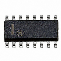
ADP3162JR-REEL ON Semiconductor, ADP3162JR-REEL Datasheet

ADP3162JR-REEL
Specifications of ADP3162JR-REEL
Available stocks
Related parts for ADP3162JR-REEL
ADP3162JR-REEL Summary of contents
Page 1
GENERAL DESCRIPTION The ADP3162 is a highly efficient dual output synchronous buck switching regulator controller optimized for converting main supply into the core supply voltage required by high-performance processors such as Tualatin. The ...
Page 2
ADP3162–SPECIFICATIONS Parameter FEEDBACK INPUT Accuracy 1.05 V Output 1.5 V Output 1.825 V Output Line Regulation Input Bias Current Crowbar Trip Threshold Crowbar Reset Threshold Crowbar Response Time FB Low Foldback Threshold REFERENCE Output Voltage Output Current VID INPUTS Input ...
Page 3
... This is a stress rating only; operation beyond these limits can cause the device to be permanently damaged. Unless otherwise specified, all voltages are referenced to GND. ORDERING GUIDE Temperature Package Model Range Description ADP3162JR 0°C to 70°C Narrow Body SOIC R-16A (SO-16) PIN CONFIGURATION VID3 1 16 VID2 2 ...
Page 4
ADP3162 –Typical Performance Characteristics 10000 1000 100 200 300 0 100 CT CAPACITOR – pF 4.10 4.05 4.00 3.95 3.90 3.85 0 250 500 750 1000 1250 OSCILLATOR FREQUENCY – kHz 400 500 ...
Page 5
ADP3162 1 VID3 VCC 16 VID2 2 REF 15 VID1 5-BIT CODE 3 CS– 14 VID0 4 PWM1 13 VID25 5 PWM2 12 COMP 6 CS PWRGD GND 9 4.7nF AD820 1.2V Table ...
Page 6
ADP3162 Cycle-by-Cycle Operation During normal operation (when the output voltage is regulated), the voltage-error amplifier and the current comparator are the main control elements. The voltage at the CT pin of the oscilla- tor ramps between 0 V and 3 ...
Page 7
The crowbar comparator releases when the output drops below the specified reset threshold, and the controller returns to normal operation if the cause of the overvoltage failure does not persist. Output Disable The ADP3162 includes ...
Page 8
ADP3162 Selecting a Standard Inductor The companies listed in Table III can provide design consul- tation and deliver power inductors optimized for high power applications upon request. Table III. Power Inductor Manufacturers Coilcraft (847) 639-6400; (800) 322-2645 http://www.coilcraft.com Coiltronics (561) ...
Page 9
V = REF R − − × − REF GNL ONL OUT − 194 . V − × mmho ...
Page 10
ADP3162 dictates whether standard threshold or logic-level threshold MOSFETs must be used. Since V < logic-level threshold GATE MOSFETs (V < 2.5 V) are strongly recommended. GS(TH) The maximum output current I determines the R O ment for ...
Page 11
LAYOUT AND COMPONENT PLACEMENT GUIDELINES The following guidelines are recommended for optimal perfor- mance of a switching regulator system. General Recommendations 1. For good results, at least a four-layer PCB is recommended. This should allow the needed ...
Page 12
ADP3162 Signal Circuitry 15. The output voltage is sensed and regulated between the FB pin and the GND pin (which connects to the signal ground plane). The output current is sensed (as a voltage) by the CS+ and CS– pins. ...


