AN8018SA-E1V Panasonic - SSG, AN8018SA-E1V Datasheet - Page 13
AN8018SA-E1V
Manufacturer Part Number
AN8018SA-E1V
Description
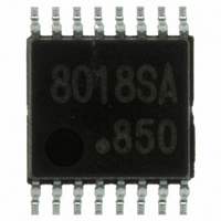
IC MULTI CONFIG ADJ 50MA 16SSOP
Manufacturer
Panasonic - SSG
Type
Step-Down (Buck), Step-Up (Boost), Invertingr
Specifications of AN8018SA-E1V
Lead Free Status
Lead free
Internal Switch(s)
No
Synchronous Rectifier
No
Number Of Outputs
2
Voltage - Output
Adj to 15V
Current - Output
50mA
Frequency - Switching
20kHz ~ 1MHz
Voltage - Input
1.8 ~ 14 V
Operating Temperature
-30°C ~ 85°C
Mounting Type
Surface Mount
Package / Case
16-SSOP
Power - Output
135mW
Other names
AN8018SAE1V
AN8018SAE1VTR
AN8018SAE1VTR
Available stocks
Company
Part Number
Manufacturer
Quantity
Price
Company:

Part Number:
AN8018SA-E1V
Manufacturer:
PANASONIC
Quantity:
1 347


I Application Notes (continued)
[4] Function descriptions
1. Reference voltage block
2. Triangular wave oscillation block
3. Error amplifier 1 block
4. Error amplifier 2 block
R1
R2
voltage. The reference voltage is stabilized when the supply voltage is 1.8 V or more. The reference voltage is also
used as the reference voltage for the error amplifier 2 block.
a peak of approximately 0.7 V and a trough of approxi-
mately 0.2 V can be generated by connecting the timing
capacitor C
The oscillation frequency can be freely set by the value of
C
tion frequency is from 20 kHz to the maximum 1 MHz.
The triangular wave is connected with the inverting input
of PWM comparator for channel 1 side and the
noninverting input of PWM comparator for channel 2 side
within the IC inside. Rough calculation of oscillation fre-
quency can be calculated by the following equation.
And refer to the experimentally determined graph of the frequency characteristics provided in the main
characteristics section.
amplified signal is input to the PWM comparator.
and a capacitor from the FB1 terminal (pin 5) to GND in series.
amplified signal is input to the PWM comparator. The internal reference voltage 1.19 V is given to the noninverting
input.
V
T
REF
and R
This block is composed of the band gap circuit, and outputs the temperature compensated 1.19 V reference
The sawtooth-waveform-like triangular wave having
f
However, boosting charge time, over-shoot and under shoot quantities are not considered in the above equation.
The output voltage of DC-DC converter is detected by the pnp-transistor-input type error-amplifier and the
Also, it is possible to perform the gain setting and the phase compensation arbitrarily by connecting a resistor
The output voltage V
The output voltage of DC-DC converter is detected by the npn-transistor-input type error-amplifier and the
OSC
R3
R4
V
≈ −
OUT1
T
V
to be connected externally. The usable oscilla-
Case of step-up output
T
OUT1
and resistor R
C
T
IN+1 3
IN−1 4
× R
=
FB2
R1 + R2
T
R2
× ln V
1
5
OUT1
Error amplifier 1
block
T
V
Figure 2. Connection method of error amplifier 1 block
to the OSC terminal (pin 1).
·
OSCL
OSCH
R3 + R4
can be set by making connection as shown in figure 2.
R4
≈ 0.8 ×
To PWM
comparator input
·
V
REF
C
SDH00008CEB
T
× R
1
T
[Hz]
R1
R2
V
V
REF
OUT1
Boosting
charge
Figure 1. Triangular wave oscillation waveform
R3
R4
V
V
t
Case of inverting output
1
OUT1
IN−1
= V
IN+1 3
IN−1 4
= − (V
FB2
Discharging
REF
t
T
2
REF
5
·
R3 + R4
Error amplifier 1
block
− V
R4
IN−1
)
To PWM
comparator input
·
R1 + R2
AN8018SA
V
V
OSCH
OSCL
R1
≈ 0.2 V
≈ 0.7 V
+ V
REF
13
Related parts for AN8018SA-E1V
Image
Part Number
Description
Manufacturer
Datasheet
Request
R


Part Number:
Description:
IC CIRCUIT PROTECTOR 1A SMINI 2P
Manufacturer:
Panasonic - SSG
Datasheet:
Part Number:
Description:
IC CIRCUIT PROTECTR .7A SMINI 2P
Manufacturer:
Panasonic - SSG
Datasheet:

Part Number:
Description:
IC CIRCUIT PROTCTR 1.2A SMINI 2P
Manufacturer:
Panasonic - SSG
Datasheet:

Part Number:
Description:
IC CIRCUIT PROTECTR 1.2A SNMP 2P
Manufacturer:
Panasonic - SSG
Datasheet:
Part Number:
Description:
IC CIRCUIT PROTECTOR 1A SNMP 2P
Manufacturer:
Panasonic - SSG
Datasheet:
Part Number:
Description:
IC CIRCUIT PROTECTR 1.8A SNMP 2P
Manufacturer:
Panasonic - SSG
Datasheet:
Part Number:
Description:
IC CIRCUIT PROTECTR 2.3A SNMP 2P
Manufacturer:
Panasonic - SSG
Datasheet:

Part Number:
Description:
DIODE ZENER DUAL 6.2V SSMINI-3
Manufacturer:
Panasonic - SSG
Datasheet:
Part Number:
Description:
DIODE ZENER DUAL 6.8V SSSMINI3P
Manufacturer:
Panasonic - SSG
Datasheet:

Part Number:
Description:
DIODE ZENER QUAD 12V SSMINI-5
Manufacturer:
Panasonic - SSG
Datasheet:
Part Number:
Description:
DIODE ZENER 15V 150MW S-MINI 2P
Manufacturer:
Panasonic - SSG
Datasheet:


Part Number:
Description:
DIODE ZENER 9.1V 150MW SSMINI-2
Manufacturer:
Panasonic - SSG
Datasheet: