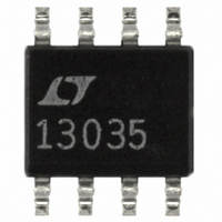
LT1303CS8-5 Linear Technology, LT1303CS8-5 Datasheet - Page 6

LT1303CS8-5
Manufacturer Part Number
LT1303CS8-5
Description
IC DC/DC CONV STEP-UP 5V 8-SOIC
Manufacturer
Linear Technology
Type
Step-Up (Boost)r
Datasheet
1.LT1303CS8-5.pdf
(12 pages)
Specifications of LT1303CS8-5
Internal Switch(s)
Yes
Synchronous Rectifier
No
Number Of Outputs
1
Voltage - Output
5V
Current - Output
200mA
Frequency - Switching
155kHz
Voltage - Input
1.8 ~ 6 V
Operating Temperature
0°C ~ 70°C
Mounting Type
Surface Mount
Package / Case
8-SOIC (3.9mm Width)
Power - Output
500mW
Lead Free Status / RoHS Status
Contains lead / RoHS non-compliant
Available stocks
Company
Part Number
Manufacturer
Quantity
Price
Company:
Part Number:
LT1303CS8-5
Manufacturer:
LT
Quantity:
10 000
Part Number:
LT1303CS8-5
Manufacturer:
LINEAR/凌特
Quantity:
20 000
Part Number:
LT1303CS8-5#PBF
Manufacturer:
LINEAR/凌特
Quantity:
20 000
Part Number:
LT1303CS8-5#TRPBF
Manufacturer:
LINEAR/凌特
Quantity:
20 000
LT1303/LT1303-5
OPERATION
6
BLOCK
Operation of the LT1303 is best understood by referring to
the Block Diagram in Figure 2. When C1’s negative input,
related to the output voltage by the appropriate resistor-
divider ratio, is higher than the 1.24V reference voltage,
C1’s output is low. C2, A3 and the oscillator are turned off,
drawing no current. Only the reference and C1 consume
current, typically 140 A. When C1’s negative input drops
below 1.24V and overcomes C1’s 6mV hysteresis, C1’s
output goes high, enabling the oscillator, current compara-
tor C2 and driver A3. Quiescent current increases to 2mA
as the device goes into active switching mode. Q1 then
turns on in controlled saturation for nominally 6 s or until
current comparator C2 trips, whichever comes first. The
switch then turns off for approximately 1.5 s, then turns on
again. The LT1303’s switching causes current to alter-
nately build up in L1 and dump into output capacitor C4 via
D1, increasing the output voltage. When the output is high
enough to cause C1’s output to go high, switching action
ceases. Capacitor C4 is left to supply current to the load
until V
the entire cycle repeats. Figure 4 details relevant wave-
forms. C1’s cycling causes low-to-mid-frequency ripple
voltage on the output. Ripple can be reduced by making the
OUT
decreases enough to force C1’s output high, and
I D AGRA
U
4
1
GND
R1
474k
R2
156k
FB
W
S
REFERENCE
1.24V
6
V
IN
5
LBI
Figure 3. LT1303-5 Block Diagram
–
+
COMPARATOR
HYSTERETIC
C1
–
+
C3
OSCILLATOR
If switch current reaches 1A, causing C2 to trip, switch on-
time is reduced and off-time increases slightly. This allows
continuous operation during bursts. C2 monitors the
voltage across 3 resistor R1 which is directly related to
the switch current. Q2’s collector current is set by the
emitter-area ratio to 0.6% of Q1’s collector current. When
R1’s voltage drop exceeds 18mV, corresponding to 1A
switch current, C2’s output goes high, truncating the on-
time portion of the oscillator cycle and increasing off-time
output capacitor large. The 100 F unit specified results in
ripple of 50mV to 100mV on the 5V output. A 220 F
capacitor will decrease ripple by approximately 50%.
COMPARATOR
OFF
2
AC COUPLED
LBO
CURRENT
100mV/DIV
5V/DIV
1A/DIV
DRIVER
V
V
OUT
SW
Figure 4. Burst Mode Operation in Action
A3
I
L
C2
SHUTDOWN
+
–
3
18mV
Q2
1
20 s/DIV
R1
3
7
8
Q1
160
PGND
SW
LT1303 F04
LT1303 BD02


