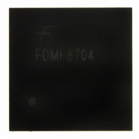
FDMF8704 Fairchild Semiconductor, FDMF8704 Datasheet - Page 9

FDMF8704
Manufacturer Part Number
FDMF8704
Description
IC MODULE DRIVER/FET 56MLP 8X8
Manufacturer
Fairchild Semiconductor
Type
Step-Down (Buck)r
Datasheet
1.FDMF8704.pdf
(11 pages)
Specifications of FDMF8704
Internal Switch(s)
Yes
Synchronous Rectifier
Yes
Number Of Outputs
1
Voltage - Output
0.8 ~ 3.2 V
Current - Output
32A
Frequency - Switching
1MHz
Voltage - Input
7 ~ 20 V
Operating Temperature
-55°C ~ 150°C
Mounting Type
Surface Mount
Package / Case
56-MLP
Power - Output
10W
Supply Voltage (min)
4.5 V
Supply Current
50 mA
Maximum Operating Temperature
+ 150 C
Mounting Style
SMD/SMT
Minimum Operating Temperature
- 55 C
Number Of Drivers
1
Lead Free Status / RoHS Status
Lead free / RoHS Compliant
Other names
FDMF8704TR
Available stocks
Company
Part Number
Manufacturer
Quantity
Price
Part Number:
FDMF8704
Manufacturer:
INTERSIL
Quantity:
20 000
FDMF8704 Rev. G
Module Power Loss Measurement and
Calculation
Refer to Figure 18 for module power loss testing method. Power
loss calculation are as follows:
(a) P
(b) P
(c) P
PCB Layout Guideline
Figure 19. shows a proper layout example of FDMF8704 and
critical parts. All of high current flow path, such as V
V
stable current flow, heat radiation and system performance.
Following is a guideline which the PCB designer should
consider:
1. Input bypass capacitors should be close to V
of FDMF8704 to help reduce input current ripple component
induced by switching operation.
OUT
LOSS
IN
OUT
and GND copper, should be short and wide for better and
= (V
= V
= P
O
IN
IN
x I
- P
x I
OUT
OUT
V
IN
IN
) + (V
(W)
PWM
Input
DISB
(W)
CIN
I
A
IN
x I
CIN
) (W)
C
Figure 18. Power Loss Measurement Block Diagram
Figure 19. Typical PCB Layout Example (Top View)
VIN
PWM
DISB
CGND PGND
VIN
IN
and GND pin
IN
VCIN
, VSWH,
VSWH
BOOT
HSEN
9
2. It is critical that the VSWH copper has minimum area for
lower switching noise emission. VSWH copper trace should
also be wide enough for high current flow. Other signal routing
path, such as PWM IN and BOOT signal, should be considered
with care to avoid noise pickup from VSWH copper area.
3. Output inductor location should be as close as possible to the
FDMF8704 for lower power loss due to copper trace.
4. Snubber for suppressing ringing and spiking of VSWH
voltage should be placed near the FDMF8704. The resistor and
capacitor need to be of proper size for power dissipation.
5. Place boot diode, ceramic bypass capacitor and boot
capacitor as close to V
to supply stable power. Routing width and length should also be
considered
6. Use multiple Vias on each copper area to interconnect each
top, inner and bottom layer to help smooth current flow and heat
conduction. Vias should be relatively large and of reasonable
inductance.
V V
C
BOOT
O
C
VCIN
I
CIN
A
L
V
C
CIN
CIN
OUT
I
OUT
and BOOT pin of FDMF8704 in order
A
V
OUT
www.fairchildsemi.com


