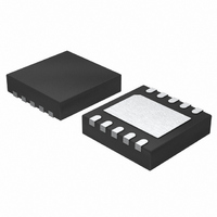
LTC3447EDD#PBF Linear Technology, LTC3447EDD#PBF Datasheet - Page 15

LTC3447EDD#PBF
Manufacturer Part Number
LTC3447EDD#PBF
Description
IC CONV DC/DC SYNC BUCK 10DFN
Manufacturer
Linear Technology
Type
Step-Down (Buck)r
Datasheet
1.LTC3447EDDPBF.pdf
(16 pages)
Specifications of LTC3447EDD#PBF
Internal Switch(s)
Yes
Synchronous Rectifier
Yes
Number Of Outputs
1
Voltage - Output
0.69 ~ 2.05 V
Current - Output
600mA
Frequency - Switching
1MHz
Voltage - Input
2.5 ~ 5.5 V
Operating Temperature
-40°C ~ 85°C
Mounting Type
Surface Mount
Package / Case
10-DFN
Lead Free Status / RoHS Status
Lead free / RoHS Compliant
Power - Output
-
Available stocks
Company
Part Number
Manufacturer
Quantity
Price
APPLICATIO S I FOR ATIO
PACKAGE DESCRIPTIO
Design Example
As a design example, assume the LTC3447 is used in a
single lithium-ion battery-powered cellular phone applica-
tion. The V
down to about 2.7V. The normal load current requirement
is a maximum of 500mA at 1.4V, but most of the time it will
be in standby mode, requiring only 200µA at 1V. Effi ciency
at both low and high load currents is important.
To ensure that the ripple currents and voltages do not
exceed desired expectations over the DAC output range,
calculations with maximum V
be used. Note that either increasing the output voltage or
decreasing V
and voltage. Choosing a maximum ripple current, ΔI
280mA, Equation 1 can be used to determine the size of
the inductor that should be used.
A 3.3µH inductor works well for this application. For best
effi ciency choose a 640mA or greater inductor with less
than 0.2Ω series resistance.
C
mately I
C
yields the following ripple voltage using Equation 3.
IN
OUT
L
will require an RMS current of at least 0.25A, approxi-
=
, selecting a 4.7µF capacitor with an ESR of 0.25Ω
(
1
LOAD(MAX)
MHz
NOTE:
1. DRAWING TO BE MADE A JEDEC PACKAGE OUTLINE M0-229 VARIATION OF (WEED-2).
2. DRAWING NOT TO SCALE
3. ALL DIMENSIONS ARE IN MILLIMETERS
3.50 ±0.05
CHECK THE LTC WEBSITE DATA SHEET FOR CURRENT STATUS OF VARIATION ASSIGNMENT
IN
2.15 ±0.05
IN
will be operating from a maximum of 4.2V
)(
1
280
will result in a decrease of ripple current
RECOMMENDED SOLDER PAD PITCH AND DIMENSIONS
/2, overtemperature (see Equation 2). For
0.25 ± 0.05
1.65 ±0.05
(2 SIDES)
mA
U
)
• .
1 4 1
U
IN
V
2.38 ±0.05
(2 SIDES)
Information furnished by Linear Technology Corporation is believed to be accurate and reliable. However,
no responsibility is assumed for its use. Linear Technology Corporation makes no representation that
the interconnection of its circuits as described herein will not infringe on existing patent rights.
⎛
⎜
⎝
and minimum V
–
1 4
W
4 2
0.50
BSC
.
.
U
V
V
0.675 ±0.05
⎞
⎟ =
⎠
PACKAGE
OUTLINE
10-Lead Plastic DFN (3mm × 3mm)
3 3
(Reference LTC DWG # 05-08-1698)
.
OUT
U
µ
(SEE NOTE 6)
H
should
TOP MARK
L
, of
PIN 1
DD Package
0.200 REF
Note that the majority of the ripple voltage is generated
by the capacitor’s ESR. Most ceramic capacitors will have
a typical ESR of 10mΩ or less. Selecting capacitors with
low ESRs will signifi cantly reduce the ripple voltage.
Effi ciency can be improved by taking advantage of the
LT3447’s Burst Mode operation. When entering the standby
mode, ensure that the burst disable bit is set to 0 when
the output voltage DAC is updated. Likewise, when enter-
ing a heavy current load mode, ensure the burst disable
bit is set to 1 when the output voltage DAC is updated.
Figure 11 shows the advantage of utilizing the Burst Mode
function.
4. DIMENSIONS OF EXPOSED PAD ON BOTTOM OF PACKAGE DO NOT INCLUDE MOLD
5. EXPOSED PAD SHALL BE SOLDER PLATED
6. SHADED AREA IS ONLY A REFERENCE FOR PIN 1 LOCATION ON THE
FLASH. MOLD FLASH, IF PRESENT, SHALL NOT EXCEED 0.15mm ON ANY SIDE
TOP AND BOTTOM OF PACKAGE
∆
70
V
mV
OUT
Figure 11. Effi ciency vs Load Current ( V
+
=
7 4
3.00 ±0.10
0.75 ±0.05
(4 SIDES)
0 280
.
.
mV
100
90
80
70
60
50
40
30
20
10
0
0.00 – 0.05
0.1
A
=
DAC(MIN)
1.65 ± 0.10
⎛
⎜
⎝
STBY
(2 SIDES)
77 4
0 25
.
1
.
LOAD CURRENT (mA)
DAC(MAX)
mV
Ω
BOTTOM VIEW—EXPOSED PAD
+
DAC(MIN)
10
5
R = 0.115
6
8 1
2.38 ±0.10
(
(2 SIDES)
TYP
MHz
NORMAL
100
DAC(MAX)
BURST
PSK
10
)( .
1
1
3447 F11
LTC3447
0.50 BSC
0.25 ± 0.05
1000
4 7
0.38 ± 0.10
IN
(DD10) DFN 1103
= 4.2V)
µ
F
)
⎞
⎟ =
⎠
15
3447f


