LT3587EUD#PBF Linear Technology, LT3587EUD#PBF Datasheet
LT3587EUD#PBF
Specifications of LT3587EUD#PBF
Available stocks


Related parts for LT3587EUD#PBF


LT3587EUD#PBF Summary of contents
Page 1
... QFN package. This high level of integration combined with small external components makes the LT3587 ideal for space constrained applications. L, LT, LTC and LTM are registered trademarks of Linear Technology Corporation. All other trademarks are the property of their respective owners. 10μF SW1 ...
Page 2
... Storage Temperature Range ................... –65°C to 125°C ORDER INFORMATION LEAD FREE FINISH TAPE AND REEL LT3587EUD#PBF LT3587EUD#TRPBF Consult LTC Marketing for parts specifi ed with wider operating temperature ranges. Consult LTC Marketing for information on non-standard lead based fi nish parts. For more information on lead free part marking, go to: For more information on tape and reel specifi ...
Page 3
ELECTRICAL CHARACTERISTICS temperature range, otherwise specifi cations are at T PARAMETER Boost1 CAP1 Bias Current FB1 Reference Voltage V Output Voltage OUT1 SW1 Current Limit SW1 V CESAT SW1 Leakage Current EN/SS1 for Full Inductor Current EN/SS1 Shutdown Voltage Threshold ...
Page 4
LT3587 TYPICAL PERFORMANCE CHARACTERISTICS Shutdown Quiescent Current vs Input Supply Voltage 3.6V VIN EN/SS1 = EN/SS3 = 0V 125°C 8 90°C 6 25°C –40° 2.5 3 3.5 4 4.5 5 5.5 INPUT VOLTAGE (V) 3587 ...
Page 5
TYPICAL PERFORMANCE CHARACTERISTICS Switching Frequency vs Temperature 1. 3.6V VIN 1.10 1.00 0.90 0.80 –50 – 100 TEMPERATURE (°C) 3587 G08 Switches Current Limit vs Duty Cycle 2 3.6V VIN 2.0 SW2 ...
Page 6
LT3587 TYPICAL PERFORMANCE CHARACTERISTICS EN/SS1, EN/SS3 Shutdown Threshold vs Temperature 0. 3.6V VIN 0.40 0.35 0.30 0.25 0.20 –50 – TEMPERATURE (°C) PIN FUNCTIONS V (Pin 1): Boost3 Output Pin. This pin is the drain of ...
Page 7
PIN FUNCTIONS V (Pin 14): Boost1 Output Pin. This pin is the drain OUT1 of an output disconnect PMOS transistor. FB1 (Pin 15): Boost1 Output Voltage Feedback Pin. Con- nect a resistor R from this pin to V FB1 such ...
Page 8
LT3587 BLOCK DIAGRAM V IN 1μA EN/SS3 REF A8 0.8V – 200mV FLT V OUT3 R VFB3 V MAX V FB3 56. EN/SS1 PTAT BIAS EN/SS3 BANDGAP OSCILLATOR AND LDO V OUT1 R FB1 ...
Page 9
OPERATION All three channels of the LT3587 use a constant frequency, current mode control scheme to provide voltage and/or current regulation at the output. Operation can be best un- derstood by referring to the Block Diagram in Figure 1. If ...
Page 10
LT3587 APPLICATIONS INFORMATION Inductor Selection A 15μH inductor and a 10μH inductor are recommended for the LT3587 Boost1 channel and Boost3 channel re- spectively. The inverting channel can use 15μH or 22μH inductors. Although small size is the major concern ...
Page 11
APPLICATIONS INFORMATION capacitance will slow down the switching waveform, which can cause signifi cant switching losses at 1MHz switch- ing frequency. Some recommended Schottky diodes are listed in Table 2. Table 2. Recommended Schottky Diodes DIODE FORWARD FORWARD CAPACI- PART ...
Page 12
LT3587 APPLICATIONS INFORMATION current Figure 4 compares the transient OUT3 LIMIT responses with and without current limit when a current overload occurs. 15V V VOUT3 5V/DIV I 20mA VOUT3 13mA/DIV LOAD STEP I L4 200mA/DIV ...
Page 13
APPLICATIONS INFORMATION Setting The Output Voltages and The Boost3 Output Current The LT3587 has a trimmed internal feedback resistor feedback resistor from each output pin to its corresponding feedback pin sets the outputs to 15V for Boost1, –8V ...
Page 14
LT3587 APPLICATIONS INFORMATION Output Disconnect Both the Boost1 and the Boost3 channels have an output disconnect between their respective CAP pin and V pin. This disconnect feature prevents a DC path from OUT For Boost1, this ...
Page 15
APPLICATIONS INFORMATION FLT B1 B3 SW3 V IN EN/SS EN/SS CAP3 V FB3 LT3587 R VFB3 V OUT3 I FB3 DN SW2 FB2 FLT B1 B3 SW3 V IN EN/SS EN/SS CAP3 R VFB3 LT3587 V FB3 V OUT3 I ...
Page 16
LT3587 APPLICATIONS INFORMATION Besides acting as a fault output indicator, the Fault pin is also an input pin. If this pin is externally forced low below 400mV, the LT3587 behaves fault event has been detected and all ...
Page 17
APPLICATIONS INFORMATION V VIN 2. 10μH V SW3 IN 1μF CAP3 LT3587 V OUT3 I EN/SS3 FB3 R IFB3 8.06k PWM FREQ 2.5V 0V Figure 13. Six White LEDs Driver With PWM Dimming I VOUT3 0mA 13mA/DIV I ...
Page 18
LT3587 APPLICATIONS INFORMATION 100 10 IDEAL 1 MEASURED 0.1 0. DUTY CYCLE (%) Figure 15. Average LED Current Variation with PWM Duty Cycle at 100Hz PWM Frequency The time it takes for the LED current to reach its ...
Page 19
APPLICATIONS INFORMATION Lower Input Voltage Applications The LT3587 can be used in lower input voltage applica- tions. The V supply voltage to the LT3587 must be IN 2.5V to 6V. However, the inductors can be run off a lower voltage. ...
Page 20
LT3587 APPLICATIONS INFORMATION Board Layout Consideration As with all switching regulators, careful attention must be paid to the PCB board layout and component placement. To maximize effi ciency, switch rise and fall times are made as short as possible. To ...
Page 21
TYPICAL APPLICATIONS Li-Ion Powered Supply for CCD Imager and Five White Backlight LEDs LED DRIVER 20mA UP TO 24V (OPTIONAL) R 8.06k C3 100nF 2. C1: MURATA GRM21BR61C106KE15L C2: MURATA GRM188R61C225KE15D C3, C5: MURATA GRM033R60J104KE19D C4: MURATA GRM21BR71E225KA73L ...
Page 22
LT3587 TYPICAL APPLICATIONS Driver For a CCD Imager and an OLED Display Panel with Soft-Start C3 100nF C1: TAIYO YUDEN TMK212BJ475KG-T C2: TAIYO YUDEN EMK107BJ225KA-T C3, C5: TAIYO YUDEN JMK063BJ104KP-F C4: TAIYO YUDEN GMK107BJ105KA-T C6: TAIYO YUDEN LMK105BJ105KV-F Extending the ...
Page 23
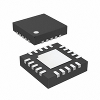
... ON THE TOP AND BOTTOM OF PACKAGE Information furnished by Linear Technology Corporation is believed to be accurate and reliable. However, no responsibility is assumed for its use. Linear Technology Corporation makes no representa- tion that the interconnection of its circuits as described herein will not infringe on existing patent rights. UD Package 20-Lead Plastic QFN (3mm × ...
Page 24
... OUT(MAX 10V 32V 6mA, I IN(MAX) OUT(MAX 40V 1mA, I < 1μA, MSOP-8E, OUT(MAX 0109 REV C • PRINTED IN USA © LINEAR TECHNOLOGY CORPORATION 2008 < 1μA, < 1μA, < 1μA, < 16μA, < 1μA, SD < 1μA, SD < 1μA, SD < 1μA, < 12μA, 3587fc ...