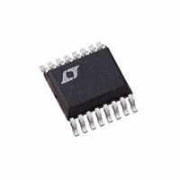
LTC3703EGN#PBF Linear Technology, LTC3703EGN#PBF Datasheet - Page 4

LTC3703EGN#PBF
Manufacturer Part Number
LTC3703EGN#PBF
Description
IC BUCK/BOOST SYNC ADJ 5A 16SSOP
Manufacturer
Linear Technology
Type
Step-Down (Buck), Step-Up (Boost)r
Datasheet
1.LTC3703EGNPBF.pdf
(32 pages)
Specifications of LTC3703EGN#PBF
Internal Switch(s)
No
Synchronous Rectifier
Yes
Number Of Outputs
1
Voltage - Output
0.8 ~ 93 V
Current - Output
5A
Frequency - Switching
100kHz ~ 600kHz
Voltage - Input
9.3 ~ 100 V
Operating Temperature
-40°C ~ 85°C
Mounting Type
Surface Mount
Package / Case
16-SSOP
Primary Input Voltage
15V
No. Of Outputs
1
Output Voltage
100V
Output Current
5A
No. Of Pins
16
Operating Temperature Range
-40°C To +85°C
Msl
MSL 1 - Unlimited
Rohs Compliant
Yes
Lead Free Status / RoHS Status
Lead free / RoHS Compliant
Power - Output
-
Available stocks
Company
Part Number
Manufacturer
Quantity
Price
LTC3703
ELECTRICAL CHARACTERISTICS
TYPICAL PERFORMANCE CHARACTERISTICS
Note 1: Stresses beyond those listed under Absolute Maximum Ratings
may cause permanent damage to the device. Exposure to any Absolute
Maximum Rating condition for extended periods may affect device
reliability and lifetime.
Note 2: The LTC3703E is guaranteed to meet performance specifi cations from
0°C to 85°C. Specifi cations over the –40°C to 85°C operating temperature
range are assured by design, characterization and correlation with statistical
process controls. The LTC3703I is guaranteed over the full –40°C to 125°C
operating junction temperature range. The LTC3703H is guaranteed over the
full –40°C to 150°C operating junction temperature range.
Note 3: T
dissipation P
4
LTC3703: T
100
3.5
3.0
2.5
2.0
1.5
1.0
0.5
95
90
85
80
75
70
0
6
0
Effi ciency vs Input Voltage
V
J
V
f = 300kHz
PULSE SKIP DISABLED
CC
is calculated from the ambient temperature T
OUT
10
D
Current vs V
= 12V
according to the following formula:
J
8
= T
20
A
INPUT VOLTAGE (V)
V
+ (P
CC
30
10
VOLTAGE (V)
D
COMP = 1.5V
40
• 100 °C/W) G Package
CC
I
OUT
Voltage
12
= 5A
50
I
V
OUT
FB
60
= 0V
= 0.5A
14
70
3703 G04
3703 G01
80
16
A
100
and power
95
90
85
80
75
70
4
3
2
1
0
–50 –25
0 0.5
Effi ciency vs Load Current
V
CC
Current vs Temperature
1.0
0
1.5
TEMPERATURE (°C)
LOAD CURRENT (A)
V
25
2.0
IN
= 15V
2.5
50
V
f = 250kHz
PULSE SKIP ENABLED
Note 4: The LTC3703 is tested in a feedback loop that servos V
reference voltage with the COMP pin forced to a voltage between 1V and 2V.
Note 5: The dynamic input supply current is higher due to the power
MOSFET gate charge being delivered at the switching frequency (Q
Note 6: Guaranteed by design. Not subject to test.
Note 7: This IC includes overtemperature protection that is intended
to protect the device during momentary overload conditions. Junction
temperature will exceed 125°C when overtemperature protection is active.
Continuous operation above the specifi ed maximum operating junction
temperature may impair device reliability.
Note 8: R
Note 9: High junction temperatures degrade operating lifetimes. Operating
lifetime at junction temperatures greater than 125°C is derated to 1000 hours.
COMP = 1.5V
OUT
V
3.0
IN
75
= 5V
= 45V
V
3.5
FB
100
DS(ON)
= 0V
V
4.0
IN
125
T
= 75V
4.5
A
3703 G02
3703 G05
guaranteed by correlation to wafer level measurement.
= 25°C unless otherwise noted.
150
5.0
50mV/DIV
2A/DIV
V
I
100
OUT
OUT
90
80
70
60
50
40
30
20
10
0
6
Load Transient Response
V
V
V
V
1A TO 5A LOAD STEP
IN
OUT
CC
CC
= 50V
Shutdown Current vs
Voltage
= 12V
8
V
CC
10
VOLTAGE (V)
50μs/DIV
12
FB
14
to the
G
• f
3703 G03
3703 G06
3703fb
OSC
16
).


