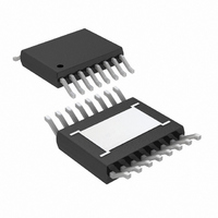
LT3500EMSE#PBF Linear Technology, LT3500EMSE#PBF Datasheet - Page 11

LT3500EMSE#PBF
Manufacturer Part Number
LT3500EMSE#PBF
Description
IC REG STEP-DOWN 2A 16-MSOP
Manufacturer
Linear Technology
Type
Step-Down (Buck)r
Datasheet
1.LT3500EDDPBF.pdf
(28 pages)
Specifications of LT3500EMSE#PBF
Topology
Step-Down (Buck) (1), Linear (LDO) (1)
Function
Any Function
Number Of Outputs
2
Frequency - Switching
500kHz ~ 2.4MHz
Voltage/current - Output 1
0.8 ~ 38.9 V, 2A
Voltage/current - Output 2
Adjustable, 13mA
W/led Driver
No
W/supervisor
No
W/sequencer
No
Voltage - Supply
3 V ~ 36 V
Operating Temperature
-40°C ~ 125°C
Mounting Type
Surface Mount
Package / Case
16-MSOP Exposed Pad
Current - Output
2A
Voltage - Output
0.8 ~ 38.9 V
Voltage - Input
3 ~ 36 V
Internal Switch(s)
Yes
Synchronous Rectifier
No
Primary Input Voltage
36V
No. Of Outputs
2
Output Current
2A
No. Of Pins
16
Operating Temperature Range
-40°C To +125°C
Msl
MSL 1 - Unlimited
Supply Voltage Range
2.4V To 36V
Rohs Compliant
Yes
Lead Free Status / RoHS Status
Lead free / RoHS Compliant
Power - Output
-
Available stocks
Company
Part Number
Manufacturer
Quantity
Price
OPERATION
V
set the soft-start latch, resulting in a complete soft-start
sequence.
The switch driver operates from either the V
age. An external diode and capacitor are used to generate
a drive voltage higher than V
and maintain high effi ciency.
In addition to the switching regulator, the LT3500 contains
a NPN linear regulator with a 0.8V reference, and 13mA
current capability. The 0.8 reference will track the SS pin
APPLICATIONS INFORMATION
Choosing the Output Voltage
The output voltage is programmed with a resistor divider
between the output and the FB pin. Choose the 1% resis-
tors according to:
R2 should be 10.0k or less to avoid bias current errors.
Reference designators refer to the Block Diagram in
Figure 1.
Choosing the Switching Frequency
The LT3500 switching frequency is set by resistor R5 in
Figure 1. The R
Setting resistor R5 sets the current in the R
which determines the oscillator frequency as illustrated
in Figure 2.
The switching frequency is typically set as high as pos-
sible to reduce overall solution size. The LT3500 employs
techniques to enhance dropout at high frequencies but
effi ciency and maximum input voltage decrease due to
switching losses and minimum switch on times. The
IN
R1= R2
undervoltage detection or thermal shutdown will
V
0.8V
OUT1
T
/SYNC pin is internally regulated at 1V.
– 1
IN
to saturate the output NPN
IN
or BST volt-
T
/SYNC pin
maximum recommended frequency can be approximated
by the equation:
where V
(D1 Figure 1), V
switch, and t
switch, all at maximum load current.
in the same manner as the switching regulator. The linear
output can also be confi gured to drive an external NPN to
provide a linear regulator with higher current capability.
A power good comparator with 30mV of hysteresis trips
when both FB and LFB are above 90% of the 0.8V refer-
ence. The PG output is an open collector NPN that is off
when the output is in regulation allowing a resistor to pull
the PG pin to a desired voltage. The PG output is an open-
collector NPN that is on when the output is in regulation
providing either drive for an output disconnect transistor
or inverted power good logic.
Frequency (Hz) =
D
Figure 2. Frequency vs R
2500
2250
2000
1750
1500
1250
1000
is the forward voltage drop of the catch diode
750
500
250
0
0
ON(MIN)
20
SW
40
is the voltage drop of the internal
V
60
IN
is the minimum on time of the
V
R
OUT1
80
− V
RT/SYNC
100
SW
+ V
120 140
(kΩ)
T
+ V
/SYNC Resistance
D
D
160
•
t
180
ON(MIN)
3500 F02
200
1
LT3500
11
3500fc


