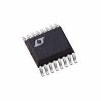
LT1766EGN#PBF Linear Technology, LT1766EGN#PBF Datasheet - Page 7

LT1766EGN#PBF
Manufacturer Part Number
LT1766EGN#PBF
Description
IC SW REG STP-DWN 200KHZ 16-SSOP
Manufacturer
Linear Technology
Type
Step-Down (Buck)r
Datasheet
1.LT1766EGNPBF.pdf
(30 pages)
Specifications of LT1766EGN#PBF
Internal Switch(s)
Yes
Synchronous Rectifier
No
Number Of Outputs
1
Voltage - Output
1.2 ~ 54 V
Current - Output
1.5A
Frequency - Switching
200kHz
Voltage - Input
5.5 ~ 60 V
Operating Temperature
-40°C ~ 125°C
Mounting Type
Surface Mount
Package / Case
16-SSOP
Primary Input Voltage
60V
No. Of Outputs
1
Output Voltage
54V
Output Current
3A
No. Of Pins
16
Operating Temperature Range
0°C To +125°C
Msl
MSL 1 - Unlimited
Supply Voltage Range
5.5V To 60V
Rohs Compliant
Yes
Lead Free Status / RoHS Status
Lead free / RoHS Compliant
Power - Output
-
Available stocks
Company
Part Number
Manufacturer
Quantity
Price
PIN FUNCTIONS
TYPICAL PERFORMANCE CHARACTERISTICS
GND (Pins 1, 8, 9, 16, 17): The GND pin connections act
as the reference for the regulated output, so load regula-
tion will suffer if the ground end of the load is not at the
same voltage as the GND pins of the IC. This condition will
occur when load current or other currents fl ow through
metal paths between the GND pins and the load ground.
Keep the paths between the GND pins and the load ground
short and use a ground plane when possible. The GND
pin also acts as a heat sink and should be soldered to a
large copper plane to reduce thermal resistance. For the
FE package, the exposed pad should be soldered to the
230
220
210
200
190
180
170
2.1
1.9
1.5
1.3
1.1
0.9
0.7
1.7
–50
–50
Switching Frequency
V
C
–25
–25
Pin Shutdown Threshold
JUNCTION TEMPERATURE (°C)
JUNCTION TEMPERATURE (°C)
0
0
25
25
50
50
75
75
100
100
125
125
1766 G10
1766 G13
150
150
450
400
350
300
250
200
150
100
7.5
7.0
6.5
6.0
5.5
5.0
50
0
0
0
Minimum Input Voltage with 5V
Output
Switch Voltage Drop
0.1 0.2 0.3 0.4 0.5 0.6 0.7 0.8 0.9 1
T
SWITCH CURRENT (A)
LOAD CURRENT (A)
J
0.5
T
= 25°C
J
= 125°C
MINIMUM INPUT
VOLTAGE TO START
MINIMUM INPUT
VOLTAGE TO RUN
copper ground plane underneath the device. (See Applica-
tions Information—Layout Considerations.)
SW (Pin 2): The switch pin is the emitter of the on-chip
power NPN switch. This pin is driven up to the input pin
voltage during switch on-time. Inductor current drives the
switch pin negative during switch off-time. Negative volt-
age is clamped with the external catch diode. Maximum
negative switch voltage allowed is – 0.8V.
NC (Pins 3, 5, 7, 13): No Connection.
T
J
= 150°C
T
1
J
= –40°C
T
A
= 25°C
1766 G11
1766 G14
1.5
600
500
400
300
200
100
LT1766/LT1766-5
45
40
35
30
25
20
15
10
0
5
0
–50
0
BOOST Pin Current
Switch Minimum On-Time
vs Temperature
T
A
= 25°C
–25
JUNCTION TEMPERATURE (°C)
0
SWITCH CURRENT (A)
0.5
25
50
75
1
100
125
1766 G12
1766 G15
1766fc
7
150
1.5


