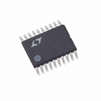
LTC3417AIFE-2#PBF Linear Technology, LTC3417AIFE-2#PBF Datasheet - Page 4

LTC3417AIFE-2#PBF
Manufacturer Part Number
LTC3417AIFE-2#PBF
Description
IC DC/DC CONV DUAL 20-TSSOP
Manufacturer
Linear Technology
Type
Step-Down (Buck)r
Datasheet
1.LTC3417AEDHC-2PBF.pdf
(20 pages)
Specifications of LTC3417AIFE-2#PBF
Internal Switch(s)
Yes
Synchronous Rectifier
Yes
Number Of Outputs
2
Voltage - Output
0.8 ~ 5 V
Current - Output
1A, 1.5A
Frequency - Switching
1.5MHz, 0.6MHz ~ 4MHz
Voltage - Input
2.25 ~ 5.5 V
Operating Temperature
-40°C ~ 125°C
Mounting Type
Surface Mount
Package / Case
20-TSSOP Exposed Pad, 20-eTSSOP, 20-HTSSOP
No. Of Outputs
2
Output Voltage
5V
Output Current
1.5A
No. Of Pins
20
Operating Temperature Range
-40°C To +125°C
Msl
MSL 1 - Unlimited
Supply Voltage Range
2.25V To 5.5V
Rohs Compliant
Yes
Lead Free Status / RoHS Status
Lead free / RoHS Compliant
Power - Output
-
Available stocks
Company
Part Number
Manufacturer
Quantity
Price
250mA/DIV
LTC3417A-2
ELECTRICAL CHARACTERISTICS
TYPICAL PERFORMANCE CHARACTERISTICS
250mA/DIV
Note 1: Stresses beyond those listed under Absolute Maximum Ratings
may cause permanent damage to the device. Exposure to any Absolute
Maximum Rating condition for extended periods may affect device
reliability and lifetime.
Note 2: The LTC3417AE-2 is guaranteed to meet specifi ed performance
from 0°C to 85°C. Specifi cations over the –40°C to 85°C operating
ambient temperature range are assured by design, characterization
and correlation with statistical process controls. The LTC3417AI-2 is
guaranteed to meet performance specifi cations over the –40°C to 125°C
operating temperature range.
Note 3: The LTC3417A-2 is tested in feedback loop which servos V
the midpoint for the error amplifi er (V
for the error amplifi er (V
Note 4: Total supply current is higher due to the internal gate charge being
delivered at the switching frequency.
4
20mV/DIV
20mV/DIV
V
V
OUT
OUT
I
I
L
L
OUT2 Burst Mode Operation
OUT1 Burst Mode Operation
V
V
I
REFER TO FIGURE 4
V
V
I
REFER TO FIGURE 4
LOAD
LOAD
IN
OUT
IN
OUT
= 3.6V
= 3.6V
= 1.8V
= 2.5V
= 100mA
= 60mA
ITH2
2μs/DIV
2μs/DIV
= 0.6V).
ITH1
= 0.6V) and V
3417A-2 G01
3417A-2 G04
250mA/DIV
250mA/DIV
20mV/DIV
20mV/DIV
FB2
V
V
OUT
OUT
to the midpoint
I
I
L
L
OUT2 Pulse Skipping
Mode Operation
OUT1 Pulse Skipping
Mode Operation
V
V
I
REFER TO FIGURE 4
LOAD
V
V
I
REFER TO FIGURE 4
IN
OUT
LOAD
IN
OUT
= 3.6V
= 3.6V
FB1
= 1.8V
= 100mA
= 2.5V
= 60mA
to
2μs/DIV
2μs/DIV
Note 5: Switch on-resistance is guaranteed by design and test correlation
on the DHC package and by fi nal test correlation on the FE package.
Note 6: Variable frequency operation with resistor is guaranteed by design
but not production tested and is subject to duty cycle limitations.
Note 7: This IC includes overtemperature protection that is intended
to protect the device during momentary overload conditions. Junction
temperature will exceed 125°C when overtemperature protection is active.
Continuous operation above the specifi ed maximum operating junction
temperature may impair device reliability.
Note 8: T
dissipation, P
J
LTC3417AEDHC-2: T
LTC3417AEFE-2: T
is calculated from the ambient temperature, T
D
, according to the following formula:
3417A-2 G02
3417A-2 G05
250mA/DIV
250mA/DIV
20mV/DIV
20mV/DIV
V
V
OUT
OUT
J
I
= T
I
L
L
J
= T
V
V
I
REFER TO FIGURE 4
OUT2 Forced Continuous
Mode Operation
OUT1 Forced Continuous
Mode Operation
A
LOAD
V
V
I
REFER TO FIGURE 4
IN
OUT
LOAD
IN
OUT
+ (P
A
= 3.6V
= 3.6V
+ (P
= 1.8V
= 100mA
= 2.5V
= 60mA
D
• 38°C/W)
D
• 43°C/W)
2μs/DIV
2μs/DIV
A
, and power
3417A-2 G03
3417A-2 G06
3417a2fa


