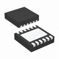
LT3500IDD#PBF Linear Technology, LT3500IDD#PBF Datasheet - Page 12

LT3500IDD#PBF
Manufacturer Part Number
LT3500IDD#PBF
Description
IC REG STP-DWN 2A 12-DFN
Manufacturer
Linear Technology
Type
Step-Down (Buck)r
Datasheet
1.LT3500EDDPBF.pdf
(28 pages)
Specifications of LT3500IDD#PBF
Topology
Step-Down (Buck) (1), Linear (LDO) (1)
Function
Any Function
Number Of Outputs
2
Frequency - Switching
500kHz ~ 2.4MHz
Voltage/current - Output 1
0.8 ~ 38.9 V, 2A
Voltage/current - Output 2
Adjustable, 13mA
W/led Driver
No
W/supervisor
No
W/sequencer
No
Voltage - Supply
3 V ~ 36 V
Operating Temperature
-40°C ~ 125°C
Mounting Type
Surface Mount
Package / Case
12-DFN
Current - Output
2A
Voltage - Output
0.8 ~ 38.9 V
Voltage - Input
3 ~ 36 V
Internal Switch(s)
Yes
Synchronous Rectifier
No
Lead Free Status / RoHS Status
Lead free / RoHS Compliant
Power - Output
-
Available stocks
Company
Part Number
Manufacturer
Quantity
Price
APPLICATIONS INFORMATION
LT3500
The following example along with the data in Table 1
illustrates the tradeoffs of switch frequency selection.
Example.
Input Voltage Range
Once the switching frequency has been determined, the
input voltage range of the regulator can be determined.
The minimum input voltage is determined by either the
LT3500’s minimum operating voltage of ~2.8V or by its
maximum duty cycle. The duty cycle is the fraction of time
that the internal switch is on during a clock cycle. The
maximum duty cycle can be determined from the clock
frequency and the minimum off time from the typical
characteristics graph.
This leads to a minimum input voltage of:
Table 1. Effi ciency and Size Comparisons for Different R
12
V
Temperature = 0°C to 85°C
t
tics
R
Frequency ≅ 820kHz
Max Frequency =
V
ON(MIN)
FREQUENCY
IN
T
IN(MIN)
/SYNC ~ 49.9k
2.5MHz
2.0MHz
1.5MHz
1.0MHz
500kHz
= 25V, V
=
= 185ns (85°C from Typical Characteris-
V
OUT1
OUT1
DC
graph), V
MAX
+ V
= 3.3V, I
25 − 0.4 + 0.6
R
T
24.9k
40.2k
90.9k
D
3.3 + 0.6
/SYNC
15k
20k
− V
D
D
OUT1
= 0.6V, V
+ V
SW
= 2.0A,
•
185ns
EFFICIENCY
SW
1
73.6
81.5
84.5
87.3
88.9
= 0.4V (85°C)
~ 835kHz
RT/SYNC
Values, V
V
IN(MAX)
12
14
18
28
36
where V
and
Figure 3 shows a typical graph of minimum input voltage
vs load current for 3.3V and 5V applications.
The maximum input voltage is determined by the absolute
maximum ratings of the V
frequency and minimum duty cycle.
The minimum duty cycle is defi ned as:
Maximum input voltage as:
DC
DC
OUT1
V
IN(MAX)
MAX
MIN
Figure 3. Minimum Input Voltage vs Load Current
= 3.3V
SW
= t
= 1 – t
8
7
6
5
4
3
2
=
ON(MIN)
is the voltage drop of the internal switch,
0
1.5μ
2.2μ
3.3μ
4.7μ
1μ
V
L
0.2 0.4 0.6 0.8
OUT1
DC
OFF(MIN)
MIN
• Frequency
+ V
LOAD CURRENT (A)
D
• Frequency.
− V
1.0
V
V
V
V
IN
OUT1
OUT1
OUT1
OUT1
D
10μ
10μ
10μ
22μ
47μ
and BST pins and by the
1.2
+ V
C
= 5V START-UP
= 5V RUNNING
= 3.3V START-UP
= 3.3V RUNNING
1.4
SW
f
L = 3.3μH
SW
1.6 1.8
= 1MHz
3500 F03
2.0
C + L AREA
(mm
24
24
24
34
40
2
)
3500fc


