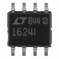
LTC1624IS8#PBF Linear Technology, LTC1624IS8#PBF Datasheet - Page 15

LTC1624IS8#PBF
Manufacturer Part Number
LTC1624IS8#PBF
Description
IC SW REG CONTROLLER N-CH 8-SOIC
Manufacturer
Linear Technology
Type
Step-Down (Buck), Step-Up (Boost), Inverting, Sepicr
Datasheet
1.LTC1624CS8PBF.pdf
(28 pages)
Specifications of LTC1624IS8#PBF
Internal Switch(s)
No
Synchronous Rectifier
No
Number Of Outputs
1
Voltage - Output
1.19 ~ 30 V
Current - Output
2A
Frequency - Switching
200kHz
Voltage - Input
3.5 ~ 36 V
Operating Temperature
-40°C ~ 85°C
Mounting Type
Surface Mount
Package / Case
8-SOIC (3.9mm Width)
Primary Input Voltage
36V
No. Of Outputs
1
Output Voltage
34.2V
Output Current
2A
No. Of Pins
8
Operating Temperature Range
-40°C To +85°C
Msl
MSL 1 - Unlimited
Supply Voltage Range
3.5V To 36V
Rohs Compliant
Yes
Lead Free Status / RoHS Status
Lead free / RoHS Compliant
Power - Output
-
Available stocks
Company
Part Number
Manufacturer
Quantity
Price
APPLICATIONS
Allowing a margin for variations in the LTC1624 (without
considering variation in R
current in the inductor, yields:
Boost Converter: Output Diode
The output diode conducts current only during the switch
off-time. Peak reverse voltage for boost converters is
equal to the regulator output voltage. Average forward
current in normal operation is equal to output current.
Remember boost converters are not short-circuit pro-
tected. Check to be sure the diode’s current rating exceeds
the maximum current set by R
as Motorola MBR130LT3 are recommended.
Boost Converter: Output Capacitors
The output capacitor is normally chosen by its effective
series resistance (ESR), because this is what determines
output ripple voltage.
Since the output capacitor’s ESR affects efficiency, use
low ESR capacitors for best performance. Boost regula-
tors have large RMS ripple current in the output capacitor
that must be rated to handle the current. The output
capacitor ripple current (RMS) is:
Output ripple is then simply: V
Boost Converter: Input Capacitors
The input capacitor of a boost converter is less critical due
to the fact that the input current waveform is triangular,
and does not contain large square wave currents as found
in the output capacitor. The input voltage source imped-
ance determines the size of the capacitor that is typically
10 F to 100 F. A low ESR is recommended although not
as critical as the output capacitor and can be on the order
of 0.3 . Input capacitor ripple current for the LTC1624
used as a boost converter is:
R
C
OUT
SENSE
I
RIPPLE RMS
I
OUT MAX
100
mV
U
I
INFORMATION
OUT
V
U
SENSE
V
OUT
IN MIN
SENSE
OUT
V
), assuming 30% ripple
OUT
V
= R
. Schottky diodes such
D
V
W
IN
ESR
V
IN
( I
L(RMS)
U
).
The input capacitor can see a very high surge current when
a battery is suddenly connected and solid tantalum capaci-
tors can fail under this condition. Be sure to specify surge
tested capacitors.
Boost Converter: Duty Cycle Limitations
The minimum on-time of 450ns sets a limit on how close
V
shooting and tripping the overvoltage comparator. Unless
very low values of inductances are used, this should never
be a problem. The maximum input voltage in continuous
mode is:
SEPIC Converter Applications
The LTC1624 is also well-suited to SEPIC (Single Ended
Primary Inductance Converter) converter applications.
The SEPIC converter shown in Figure 7 uses two induc-
tors. The advantage of the SEPIC converter is the input
voltage may be higher or lower than the output voltage.
The first inductor L1 together with the main N-channel
MOSFET switch resemble a boost converter. The second
inductor L2 and output diode D1 resemble a flyback or
buck-boost converter. The two inductors L1 and L2 can be
independent but also can be wound on the same core since
IN
C
V
can approach V
IN
IN(MAX)
LTC1624
I
GND
RIPPLE
V
IN
SENSE
BOOST
= 0.91V
SW
TG
–
0 3
Figure 7. SEPIC Converter
200
OUT
OUT
C
V
B
kHz L V
IN
without the output voltage over-
+ 0.5V
V
V
IN
OUT
R
M1
L1
SENSE
+
C1
OUT
+
V
For DC = 9%
IN
L2
V
C
FB
IN
D1
LTC1624
R2
R1
+
15
C
1624 F07
OUT
V
OUT


