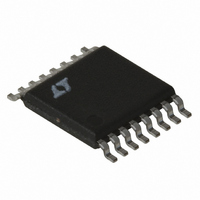
LT1765EFE-5#PBF Linear Technology, LT1765EFE-5#PBF Datasheet - Page 7

LT1765EFE-5#PBF
Manufacturer Part Number
LT1765EFE-5#PBF
Description
IC REG SW STEPDOWN 3A 16-TSSOP
Manufacturer
Linear Technology
Type
Step-Down (Buck)r
Datasheet
1.LT1765ES8PBF.pdf
(20 pages)
Specifications of LT1765EFE-5#PBF
Internal Switch(s)
Yes
Synchronous Rectifier
No
Number Of Outputs
1
Voltage - Output
5V
Current - Output
3A
Frequency - Switching
1.25MHz
Voltage - Input
3 ~ 25 V
Operating Temperature
-40°C ~ 125°C
Mounting Type
Surface Mount
Package / Case
16-TSSOP Exposed Pad, 16-eTSSOP, 16-HTSSOP
Primary Input Voltage
15V
No. Of Outputs
1
Output Voltage
5V
Output Current
6A
No. Of Pins
16
Operating Temperature Range
-40°C To +125°C
Msl
MSL 1 - Unlimited
Supply Voltage Range
3V To 25V
Rohs Compliant
Yes
Lead Free Status / RoHS Status
Lead free / RoHS Compliant
Power - Output
-
Available stocks
Company
Part Number
Manufacturer
Quantity
Price
BLOCK DIAGRAM
The LT1765 is a constant frequency, current mode buck
converter. This means that there is an internal clock and
two feedback loops that control the duty cycle of the power
switch. In addition to the normal error amplifi er, there is a
current sense amplifi er that monitors switch current on a
cycle-by-cycle basis. A switch cycle starts with an oscillator
pulse which sets the R
switch current reaches a level set by the inverting input of
the comparator, the fl ip-fl op is reset and the switch turns
off. Output voltage control is obtained by using the output
of the error amplifi er to set the switch current trip point.
This technique means that the error amplifi er commands
current to be delivered to the output rather than voltage.
A voltage fed system will have low phase shift up to the
INPUT
SHDN
SYNC
COMPARATOR
SHUTDOWN
REGULATOR
+
2.5V BIAS
3μA
S
1.33V
fl ip-fl op to turn the switch on. When
–
INTERNAL
V
CC
SLOPE COMP
OSCILLATOR
7μA
INTERNAL
V
1.25MHz
CC
+
0.005Ω
Figure 1. Block Diagram
∑
V
0.4V
–
C
+
–
CURRENT
SENSE
AMPLIFIER
VOLTAGE GAIN = 40
CURRENT
COMPARATOR
resonant frequency of the inductor and output capacitor,
then an abrupt 180° shift will occur. The current fed system
will have 90° phase shift at a much lower frequency, but
will not have the additional 90° shift until well beyond
the LC resonant frequency. This makes it much easier to
frequency compensate the feedback loop and also gives
much quicker transient response.
High switch effi ciency is attained by using the BOOST pin
to provide a voltage to the switch driver which is higher
than the input voltage, allowing the switch to be saturated.
This boosted voltage is generated with an external capacitor
and diode. A comparator connected to the shutdown pin
disables the internal regulator, reducing supply current.
LT1765/LT1765-1.8/LT1765-2.5/
S
R
g
m
FLIP-FLOP
AMPLIFIER
= 850μMho
R
S
ERROR
LT1765-3.3/LT1765-5
DO NOT FORWARD BIAS
PARASITIC DIODES
–
+
CIRCUITRY
DRIVER
1.2V
BOOST
Q1
POWER
SWITCH
1765 F01
GND
V
FB
SW
1765fd
7


