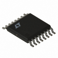
LT3431EFE#PBF Linear Technology, LT3431EFE#PBF Datasheet - Page 8

LT3431EFE#PBF
Manufacturer Part Number
LT3431EFE#PBF
Description
IC SW REG STEP-DOWN 3A 16TSSOP
Manufacturer
Linear Technology
Type
Step-Down (Buck)r
Datasheet
1.LT3431EFEPBF.pdf
(28 pages)
Specifications of LT3431EFE#PBF
Internal Switch(s)
Yes
Synchronous Rectifier
No
Number Of Outputs
1
Voltage - Output
1.2 ~ 48 V
Current - Output
3A
Frequency - Switching
500kHz
Voltage - Input
5.5 ~ 60 V
Operating Temperature
-40°C ~ 125°C
Mounting Type
Surface Mount
Package / Case
16-TSSOP Exposed Pad, 16-eTSSOP, 16-HTSSOP
Primary Input Voltage
60V
No. Of Outputs
1
Output Voltage
48V
Output Current
6.5A
No. Of Pins
16
Operating Temperature Range
-40°C To +125°C
Msl
MSL 1 - Unlimited
Rohs Compliant
Yes
Lead Free Status / RoHS Status
Lead free / RoHS Compliant
Power - Output
-
Available stocks
Company
Part Number
Manufacturer
Quantity
Price
LT3431
APPLICATIO S I FOR ATIO
FEEDBACK PIN FUNCTIONS
The feedback (FB) pin on the LT3431 is used to set output
voltage and provide several overload protection features.
The first part of this section deals with selecting resistors
to set output voltage and the second part talks about
foldback frequency and current limiting created by the FB
pin. Please read both parts before committing to a final
design.
The suggested value for the output divider resistor (see
Figure 2) from FB to ground (R2) is 5k or less, and a
formula for R1 is shown below. The output voltage error
caused by ignoring the input bias current on the FB pin is
less than 0.25% with R2 = 5k. A table of standard 1%
values is shown in Table 1 for common output voltages.
Please read the following if divider resistors are increased
above the suggested values.
Table 1
More Than Just Voltage Feedback
The feedback pin is used for more than just output voltage
sensing. It also reduces switching frequency and current
limit when output voltage is very low (see the Frequency
Foldback graph in Typical Performance Characteristics).
This is done to control power dissipation in both the IC and
in the external diode and inductor during short-circuit
conditions. A shorted output requires the switching regu-
lator to operate at very low duty cycles, and the average
current through the diode and inductor is equal to the
8
VOLTAGE
OUTPUT
R
3.3
(V)
1
10
12
15
3
5
6
8
R V
2
OUT
1 22
(k )
4.99
4.99
4.99
4.75
4.47
4.32
4.12
4.12
R2
.
U
1 22
.
(NEAREST 1%)
U
(k )
7.32
8.45
15.4
18.7
24.9
30.9
36.5
46.4
R1
W
% ERROR AT OUTPUT
DUE TO DISCREET 1%
RESISTOR STEPS
+ 0.32
– 0.43
– 0.30
+ 0.40
+ 0.20
– 0.54
+ 0.24
– 0.27
U
short-circuit current limit of the switch (typically 4A for the
LT3431, folding back to less than 2A). Minimum switch on
time limitations would prevent the switcher from attaining
a sufficiently low duty cycle if switching frequency were
maintained at 500kHz, so frequency is reduced by about
5:1 when the feedback pin voltage drops below 0.8V (see
Frequency Foldback graph). This does not affect operation
with normal load conditions; one simply sees a gear shift
in switching frequency during start-up as the output
voltage rises.
In addition to lower switching frequency, the LT3431 also
operates at lower switch current limit when the feedback
pin voltage drops below 0.6V. Q2 in Figure 2 performs this
function by clamping the V
normal 2.1V upper clamp level. This foldback current limit
greatly reduces power dissipation in the IC, diode and in-
ductor during short-circuit conditions. External synchro-
nization is also disabled to prevent interference with fold-
back operation. Again, it is nearly transparent to the user
under normal load conditions. The only loads that may be
affected are current source loads which maintain full load
current with output voltage less than 50% of final value. In
these rare situations the feedback pin can be clamped above
0.6V with an external diode to defeat foldback current limit.
Caution: clamping the feedback pin means that frequency
shifting will also be defeated, so a combination of high in-
put voltage and dead shorted output may cause the LT3431
to lose control of current limit.
The internal circuitry which forces reduced switching
frequency also causes current to flow out of the feedback
pin when output voltage is low. The equivalent circuitry is
shown in Figure 2. Q1 is completely off during normal
operation. If the FB pin falls below 0.8V, Q1 begins to
conduct current and reduces frequency at the rate of
approximately 3.5kHz/ A. To ensure adequate frequency
foldback (under worst-case short-circuit conditions), the
external divider Thevinin resistance must be low enough
to pull 115 A out of the FB pin with 0.44V on the pin (R
current limit are affected by output voltage divider imped-
ance. Although divider impedance is not critical, caution
should be used if resistors are increased beyond the
suggested values and short-circuit conditions can possi-
bly occur with high input voltage. High frequency pickup
3.8k). The net result is that reductions in frequency and
C
pin to a voltage less than its
sn3431 3431fs
DIV


