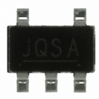
S-8354A33MC-JQST2G Seiko Instruments, S-8354A33MC-JQST2G Datasheet - Page 23

S-8354A33MC-JQST2G
Manufacturer Part Number
S-8354A33MC-JQST2G
Description
IC SWITCHING REG 3.3V SOT-23-5
Manufacturer
Seiko Instruments
Type
Step-Up (Boost)r
Datasheet
1.S-8354A33MC-JQST2G.pdf
(49 pages)
Specifications of S-8354A33MC-JQST2G
Internal Switch(s)
Yes
Synchronous Rectifier
No
Number Of Outputs
1
Voltage - Output
3.3V
Frequency - Switching
50kHz
Voltage - Input
0.9 ~ 10 V
Operating Temperature
-40°C ~ 85°C
Mounting Type
Surface Mount
Package / Case
SOT-23-5, SC-74A, SOT-25
Power - Output
250mW
Output Voltage
3.3 V
Input Voltage
10 V
Duty Cycle (max)
90 %
Switching Frequency
50 KHz
Mounting Style
SMD/SMT
Primary Input Voltage
3.8V
No. Of Outputs
1
Output Current
231mA
No. Of Pins
5
Operating Temperature Range
-40°C To +85°C
Operating Temperature Min
85°C
Rohs Compliant
Yes
Lead Free Status / RoHS Status
Lead free / RoHS Compliant
Current - Output
-
Lead Free Status / Rohs Status
Lead free / RoHS Compliant
Other names
728-1035-2
Available stocks
Company
Part Number
Manufacturer
Quantity
Price
Part Number:
S-8354A33MC-JQST2G
Manufacturer:
SEIKO/精工
Quantity:
20 000
Rev.3.0
STEP-UP, PWM CONTROL or PWM / PFM SWITCHABLE BUILT-IN TRANSISTOR SWITCHING REGULATOR
(3) S-8353DxxMC, S-8353JxxMC, S-8354DxxMC, S-8354JxxMC
Remark The power supply for the IC chip is from the VOUT pin.
Caution
_00
The Above connection diagram will not guarantee successful operation.
evaluation using the actual application to set the constant.
V
IN
C
+
−
IN
L
CONT
Soft start built-in
reference power
Oscillation circuit
PWM control circuit
Seiko Instruments Inc.
switching control
supply
or PWM / PFM
SD
circuit
Figure 15
VDD
compensating
Phase
circuit
IC internal
power
supply
+
−
S-8353/8354 Series
VOUT
VSS
C
C
R
Perform through
R
A
B
+
−
C
L
23


