XCL206B183AR-G Torex Semiconductor Ltd, XCL206B183AR-G Datasheet
XCL206B183AR-G
Specifications of XCL206B183AR-G
Available stocks


Related parts for XCL206B183AR-G


XCL206B183AR-G Summary of contents
Page 1
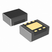
XCL205/XCL206/XCL207 Inductor Built-in Step-Down “micro DC/DC” Converters GENERAL DESCRIPTION The XCL205/XCL206/XCL207 series is a synchronous step-down micro DC/DC converter which integrates an inductor and a control IC in one tiny package (2.5mm 2.0mm, H=1.0mm). A stable power supply with an ...
Page 2
XCL205/XCL206/XCL207 PIN CONFIGURATION PIN ASSIGNMENT PIN NUMBER 1 2 PRODUCT CLASSIFICATION Ordering Information (*1) XCL205 - Fixed PWM control (*1) XCL206 - PWM / PFM automatic switching control (*1) XCL207 - Manual Mode Selection Pin ...
Page 3
BLOCK DIAGRAM XCL205A / XCL206A / XCL207A series NOTE: The XCL205 offers a fixed PWM control, a signal from CE/MODE Control Logic to PWM/PFM Selector is fixed to "L" level inside. The XCL206 control scheme is PWM/PFM automatic switching, a ...
Page 4
XCL205/XCL206/XCL207 ELECTRICAL CHARACTERISTICS XCL205A123AR/XCL206A123AR/XCL207A123AR, V PARAMETER SYMBOL Output Voltage V OUT Operating Voltage Range V IN Maximum Output Current I OUTMAX UVLO Voltage V UVLO Supply Current (XCL205 Supply Current (XCL206, XCL207) Stand-by Current I STB Oscillation Frequency ...
Page 5
ELECTRICAL CHARACTERISTICS (Continued) XCL205A183AR/XCL206A183AR/XCL207A183AR, V PARAMETER SYMBOL Output Voltage V OUT Operating Voltage Range V IN Maximum Output Current I OUTMAX UVLO Voltage V UVLO Supply Current (XCL205 Supply Current (XCL206, XCL207) Stand-by Current I STB Oscillation Frequency ...
Page 6
XCL205/XCL206/XCL207 ELECTRICAL CHARACTERISTICS (Continued) XCL205B123AR/XCL206B123AR/ XCL207B123AR, V PARAMETER SYMBOL Output Voltage V OUT Operating Voltage Range V IN Maximum Output Current I OUTMAX UVLO Voltage V UVLO Supply Current (XCL205 Supply Current (XCL206, XCL207) Stand-by Current I STB ...
Page 7
ELECTRICAL CHARACTERISTICS (Continued) XCL205 B183AR/XCL206 B183AR/ XCL207B183AR, V PARAMETER SYMBOL Output Voltage V OUT Operating Voltage Range V IN Maximum Output Current I OUTMAX UVLO Voltage V UVLO Supply Current (XCL205 Supply Current (XCL206, XCL207) Stand-by Current I ...
Page 8
XCL205/XCL206/XCL207 ELECTRICAL CHARACTERISTICS (Continued) XCL205C123AR/XCL206C123AR/ XCL207C123AR, V PARAMETER SYMBOL Output Voltage V OUT Operating Voltage Range V IN Maximum Output Current I OUTMAX UVLO Voltage V UVLO Supply Current (XCL205 Supply Current (XCL206, XCL207) Stand-by Current I STB ...
Page 9
ELECTRICAL CHARACTERISTICS (Continued) XCL205C183AR/XCL206C183AR/ XCL207C183AR, V PARAMETER SYMBOL Output Voltage V OUT Operating Voltage Range V IN Maximum Output Current I OUTMAX UVLO Voltage V UVLO Supply Current (XCL205 Supply Current (XCL206, XCL207) Stand-by Current I STB Oscillation ...
Page 10
XCL205/XCL206/XCL207 ELECTRICAL CHARACTERISTICS (Continued) PFM Switching Current ( Nominal Output Voltage (XCL206/XCL207 Series) PFM NOMINAL OUTPUT VOLTAGE MIN. 0.8V V 1.2V 190mA OUT(T) 1.2V V 1.8V 180mA OUT(T) 1.8V V 4.0V 170mA OUT(T) Input Voltage (V ) for ...
Page 11
OPERATIONAL DESCRIPTION The XCL205/XCL/206/XCL207 series consists of a reference voltage source, ramp wave circuit, error amplifier, PWM comparator, phase compensation circuit, output voltage adjustment resistors, P-channel MOSFET driver transistor, N-channel MOSFET switching transistor for the synchronous switch, current limiter circuit, ...
Page 12
XCL205/XCL206/XCL207 OPERATIONAL DESCRIPTION (Continued) <Short-Circuit Protection> The short-circuit protection circuit monitors the internal R1 and R2 divider voltage from the V block diagram shown in the previous page). In case where output is accidentally shorted to the Ground and when ...
Page 13
OPERATIONAL DESCRIPTION (Continued) C High Speed Discharge L The XCL205B(C)/ XCL206B(C)/ XCL207B(C) series can quickly discharge the electric charge at the output capacitor (C low signal to the CE pin which enables a whole IC circuit put into OFF state, ...
Page 14
XCL205/XCL206/XCL207 OPERATIONAL DESCRIPTION (Continued) <CE/MODE Pin Function> The operation of the XCL205/XCL206/ XCL207 series will enter into the shut down mode when a low level signal is input to the CE/MODE pin. During the shutdown mode, the current consumption of ...
Page 15
OPERATIONAL DESCRIPTION (Continued) Soft Start The XCL205/XCL206/XCL207 series (A series and C series) provide 0.9ms (TYP). The XCL205B/XCL206B/XCL207B series provide 0.32ms (TYP) however, when V reach 90% of the output nominal voltage when the CE pin is turned on. V ...
Page 16
XCL205/XCL206/XCL207 NOTE ON USE 1. The XCL205/XCL206/XCL207 series is designed for use with ceramic output capacitors. If, however, the potential difference is too large between the input voltage and the output voltage, a ceramic capacitor may fail to absorb the ...
Page 17
NOTE ON USE (Continued) 14. In order to stabilize V voltage level and oscillation frequency, we recommend that a by-pass capacitor (C IN connected as close as possible to the V 15. High step-down ratio and very light load may ...
Page 18
XCL205/XCL206/XCL207 NOTE ON USE (Continued) Instructions of pattern layouts 1. In order to stabilize V voltage level, we recommend that a by-pass capacitor ( (No.6) & V (No.5) pins Please mount each external component as ...
Page 19
TEST CIRCUITS XCL205/XCL206/XCL207 Series 19/26 ...
Page 20
XCL205/XCL206/XCL207 TYPICAL PERFORMANCE CHARACTERISTICS (1) Efficiency vs. Output Current XCL205A183AR/XCL206A183AR/XCL207A183AR 100 XCL206/XCL207(PWM/PFM 2.4V 3.6V 40 VIN= 4.2V XCL205/XCL207 Output Current:I (3) Ripple Voltage vs. Output Current XCL205A183AR/XCL206A183AR/XCL207A183AR 100 80 60 XCL205/XCL207 (PWM) 40 ...
Page 21
TYPICAL PERFORMANCE CHARACTERISTICS (Continued) (7) UVLO Voltage vs. Ambient Temperature XCL205A183AR/XCL206A183AR/XCL207A183AR 1.8 1.5 1.2 0.9 0.6 0.3 0.0 -50 - Ambient Temperature (9) CE "L" Voltage vs. Ambient Temperature XCL205A183AR/XCL206A183AR/XCL207A183AR 1.0 0.9 0.8 VIN=5.0V 0.7 ...
Page 22
XCL205/XCL206/XCL207 TYPICAL PERFORMANCE CHARACTERISTICS (Continued) (13) Soft-Start Time vs. Ambient Temperature XCL205B333AR/XCL206B333AR/XCL207B333AR 500 400 300 200 100 0 -50 - Ambient Temperature (15) Load Transient Response MODE PWM/PFM Automatic Switching Control XCL206A183AR/XCL207A183AR Time:100 s/div Time: ...
Page 23
TYPICAL PERFORMANCE CHARACTERISTICS (Continued) (15) Load Transient Response (Continued) MODE PWM Control XCL205A183AR/XCL207A183AR Time:100 s/div Time: 100 s /div XCL205A183AR/XCL207A183AR Time:100 s/div Time: 100 s /div XCL205/XCL206/XCL207 Series XCL205A183AR/XCL207A183AR Time:100 s/div Time: 100 s /div XCL205A183AR/XCL207A183AR Time:100 s/div Time: 100 ...
Page 24
XCL205/XCL206/XCL207 PACKAGING INFORMATION XCL205/XCL206/XCL207 Reference Pattern Layout 24/26 Series External Lead Reference Metal Mask Design ...
Page 25
MARKING RULE XCL205/XCL206/XCL207 represents products series MARK PRODUCT SERIES 4 XCL205A*****-G C XCL205B*****-G K XCL205C*****-G 5 XCL206A*****-G D XCL206B*****-G L XCL206C*****-G 6 XCL207A*****-G E XCL207B*****-G M XCL207C*****-G represents type of DC/DC converters OUTPUT VOLTAGE (V) OCSILLATION FREQUENCY=3.0MHz 0.x 1.x 2.x ...
Page 26
... Should you wish to use the products under conditions exceeding the specifications, please consult us or our representatives assume no responsibility for damage or loss due to abnormal use. 7. All rights reserved. No part of this datasheet may be copied or reproduced without the prior permission of TOREX SEMICONDUCTOR LTD. 26/26 Series ...