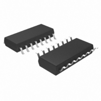
MB3759PF-G-BND-JNE1 Fujitsu Semiconductor America Inc, MB3759PF-G-BND-JNE1 Datasheet

MB3759PF-G-BND-JNE1
Specifications of MB3759PF-G-BND-JNE1
Related parts for MB3759PF-G-BND-JNE1
MB3759PF-G-BND-JNE1 Summary of contents
Page 1
FUJITSU SEMICONDUCTOR DATA SHEET ASSP For Power Management Applications Switching Regulator Controller (Switchable between push-pull and single-end functions) MB3759 DESCRIPTION The MB3759 is a control IC for constant-frequency pulse width modulated switching regulators. The IC contains most of the functions ...
Page 2
MB3759 PIN ASSIGNMENT BLOCK DIAGRAM 0.2 V Dead time DT 4 control Error amp.1 1 IN1 2 IN1 IN2 16 IN2 15 Error amp Feed back 2 (TOP VIEW) IN1 1 ...
Page 3
ABSOLUTE MAXIMUM RATINGS Parameter Power supply voltage Collector output voltage Collector output current Amplifier input voltage Plastic DIP Power dissipation SOP * Operating temperature Storage temperature *: When mounted square double-sided epoxy circuit board (1.5 mm ...
Page 4
MB3759 ELECTRICAL CHARACTERISTICS Parameter Output voltage Input regulation Load regulation Reference Temperature stability section Short circuit output current Reference lockout voltage Reference hysteresis voltage Oscillator frequency Standard deviation of frequency Oscillator section Frequency change with voltage Frequency change with temperature ...
Page 5
Parameter Input offset voltage Input offset current Input bias current Common-mode input voltage Open-loop voltage Error amplification amplifier section Unity-gain bandwidth Common-mode rejection ratio ISINK Output sink current (pin 3) ISOURCE Collector leakage current Emitter leakage current Output Emitter ...
Page 6
MB3759 TEST CIRCUIT TEST INPUT OPERATING TIMING = 3 Voltage OUTPUT 1 OUTPUT 15V CC 150 /2 W 150 ...
Page 7
OSCILLATION FREQUENCY f = OSC OUTPUT LOGIC TABLE Input (Output Control) GND V REF 1.2 · µF T fosc : kH Z Output State Single-ended or parallel output Push-pull MB3759 ...
Page 8
MB3759 TYPICAL CHARACTERISTICS Reference voltage vs. power supply voltage REF 4 V REF Power supply voltage V Oscillator vs 500 k 200 k 100 k 50 ...
Page 9
Open loop voltage amplification vs. frequency 100 100 100 Frequency f (H ...
Page 10
MB3759 (Continued) Output voltage vs. reference voltage 400 OUT Reference voltage V Power dissipation vs. power supply voltage 1000 Ta = +25 C 800 600 ...
Page 11
BASIC OPERATION Switching regulators can achieve a high level of efficiency. This section describes the basic principles of operation using a chopper regulator as an example. As shown in the diagram, diode D provides a current path for the current ...
Page 12
MB3759 SWITCHING ELEMENT 1. Selection of the Switching Transistor It can be said that the success or otherwise of a switching regulator is determined by the choice of switching transistor. Typically, the following parameters are considered in selecting a transistor. ...
Page 13
The figure below shows an example of the ASO characteristics for a forward-biased power transistor (2SC3058A) suitable for switching. Check that the ASO characteristics for the transistor you intend to use fully covers the load curve. Next, check whether the ...
Page 14
MB3759 APPLICATION IN PRACTICAL CIRCUITS 1. Error Amplifier Gain Adjustment Take care that the bias current does not become large when connecting an external circuit to the FB pin (pin 3) for adjusting the amplifier gain. As the FB pin ...
Page 15
Soft Start A soft start function can be incorporated by using the dead-time control element Setting the dead-time When the power is turned on not yet charged and the DT input is pulled to the ...
Page 16
MB3759 • Initial limit current I L1 The condition for V is the diode is reverse biased ...
Page 17
(2) Example that does not use a diode V REF The output current I after current limiting is ...
Page 18
MB3759 (3) When an external stabilized negative power supply is presen The output current I after current limiting is – ...
Page 19
Example Power Supply Voltage Supply Circuit (1) Supplied via a Zener diode (2) Supplied via a three-terminal regulator AC 6. Example Protection Circuit for Output Transistor Due to ...
Page 20
MB3759 (2) Provide a bias at the anode-side of the diode to clamp the low level side of the transistor. (3) Drive the transformer via a buffer transistor 7 0.7 V 0.1 µF 1.2 ...
Page 21
Typical Application (1)Chopper regulator 1 AC 100 100 k 0. 5 ...
Page 22
MB3759 (2) Inverter regulator AC 100 100 k 0.22 µF 2 µ 5.1 k 5.1 k 300 ...
Page 23
... The worker must put on a grounding device containing 250 k • Do not apply a negative voltage - Applying a negative voltage of 0 less to an LSI may generate a parasitic transistor, resulting in malfunction. ORDERING INFORMATION Part number MB3759P MB3759PF resistors in series. Package 16-pin plastic DIP (DIP-16P-M04) 16-pin plastic SOP (FPT-16P-M06) ...
Page 24
MB3759 PACKAGE DIMENSIONS 16-pin plastic DIP (DIP-16P-M04) INDEX-1 INDEX-2 4.36(.172)MAX 3.00(.118)MIN +0.30 0.99 –0 +.012 .039 –0 1.27(.050) MAX 1994 FUJITSU LIMITED D16033S-2C +0.20 19.55 –0.30 +.008 .770 –.012 6.20±0.25 (.244±.010) 0.51(.020)MIN 0.25±0.05 (.010±.002) 0.46±0.08 (.018±.003) +0.30 1.52 ...
Page 25
SOP (FPT-16P-M06) +0.25 +.010 * 1 10.15 .400 –0.20 –.008 16 INDEX 1 1.27(.050) 0.47±0.08 (.019±.003) 0.10(.004) 0.10(.004) 2002 FUJITSU LIMITED F16015S-c-4-7 C Note These dimensions include resin protrusion. Note These ...
Page 26
MB3759 FUJITSU LIMITED All Rights Reserved. The contents of this document are subject to change without notice. Customers are advised to consult with FUJITSU sales representatives before ordering. The information, such as descriptions of function and application circuit examples, in ...


