SC470ITSTRT Semtech, SC470ITSTRT Datasheet - Page 11
SC470ITSTRT
Manufacturer Part Number
SC470ITSTRT
Description
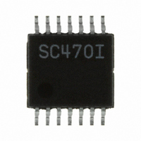
IC SYNC BUCK CONTROLLER 14-TSSOP
Manufacturer
Semtech
Type
Step-Down (Buck)r
Datasheet
1.SC470IMLTRT.pdf
(31 pages)
Specifications of SC470ITSTRT
Internal Switch(s)
No
Synchronous Rectifier
No
Number Of Outputs
1
Voltage - Output
0.5 ~ 25 V
Voltage - Input
1.8 ~ 25 V
Operating Temperature
0°C ~ 85°C
Mounting Type
Surface Mount
Package / Case
14-TSSOP
Lead Free Status / RoHS Status
Lead free / RoHS Compliant
Current - Output
-
Power - Output
-
Frequency - Switching
-
Other names
SC470ITSTR
Available stocks
Company
Part Number
Manufacturer
Quantity
Price

Part Number:
SC470ITSTRT
Manufacturer:
SEMTECH/美国升特
Quantity:
20 000


(maximum) minimum off-time one-shot. For best dropout
performance, use the slowest on-time setting of 200kHz.
When working with low input voltages, the duty-factor
limit must be calculated using worst-case values for on
and off times. The IC duty-factor limitation is given by:
Be sure to include inductor resistance and MOSFET on-
state voltage drops when performing worst-case dropout
duty-factor calculations.
470 System DC Accuracy
Two IC parameters affect system DC accuracy, the error
comparator threshold voltage variation and the switching
frequency variation with line and load. The error
comparator threshold does not drift significantly with
supply and temperature. Thus, the error comparator
contributes 0.85% or less to DC system inaccuracy.
Board components and layout also influence DC
accuracy. The use of 1% feedback resistors contribute
1%. If tighter DC accuracy is required use 0.1% feedback
resistors.
The on-pulse in the SC470 is calculated to give a pseudo-
fixed frequency. Nevertheless, some frequency variation
with line and load can be expected. This variation changes
the output ripple voltage. Because constant on-
regulators regulate to the valley of the output ripple, ½
of the output ripple appears as a DC regulation error.
For example, if the feedback resistors are chosen to
divide down the output by a factor of five, the valley of
the output ripple will be VOUT. For example: if VOUT is
2.5V and the ripple is 50mV with VBAT = 6V, then the
measured DC output will be 2.525V. If the ripple increases
to 80mV with VBAT = 25V, then the measured DC output
will be 2.540V.
The output inductor value may change with current. This
will change the output ripple and thus the DC output
voltage. It will not change the frequency.
Switching frequency variation with load can be minimized
by choosing MOSFETs with lower R
MOSFETs will cause the switching frequency to increase
as the load current increases. This will reduce the ripple
and thus the DC output voltage.
POWER MANAGEMENT
Application Information (Cont.)
2005 Semtech Corp.
DUTY
t
ON
(
MIN
t
ON
)
(
MIN
t
OFF
)
(
MAX
NOT RECOMMENDED FOR NEW DESIGN
)
DS(ON)
. High R
DS(ON)
11
Design Procedure
Prior to designing an output and making component
selections, it is necessary to determine the input voltage
range and the output voltage specifications. For purposes
of demonstrating the procedure the output for the
schematic in Figure 8 on Page 17 will be designed.
The maximum input voltage (V
the highest AC adaptor voltage. The minimum input
voltage (V
voltage after accounting for voltage drops due to
connectors, fuses and battery selector switches. For the
purposes of this design we will use a V
20V.
Four parameters are needed for the output:
1) Nominal output voltage, V
2) Static (or DC) tolerance, TOL
3) Transient tolerance, TOL
will use +/-8% for purposes of this demonstration).
4) Maximum output current, I
Switching frequency determines the trade-off between
size and efficiency. Increased frequency increases the
switching losses in the MOSFETs, since losses are a
function of VIN
budget for MOSFET switches usually dictates where the
design ends up. A default R
as a starting point, but this is not set in stone. The first
thing to do is to calculate the on-time, t
V
and,
From these values of t
switching frequency as follows:
t
t
ON
ON
BAT(MAX)
_
_
VBAT
VBAT
For V
(
(
, since this depends only upon V
MIN
MAX
)
)
OUT
BAT(MIN)
3
3
< 3.3V:
3 .
3 .
2
, knowing the maximum input voltage and
) is determined by the lowest battery
10
10
12
12
R
R
ON
tON
tON
we can calculate the nominal
tON
TR
OUT
37
37
OUT
value of 1M is suggested
and size of transient (we
ST
BAT(MAX)
(we will use 1.2V).
10
10
(we will design for 6A).
(we will use +/-4%).
3
3
) is determined by
V
V
BAT
BAT
BAT
V
V
ON
BAT
OUT
OUT
www.semtech.com
, at V
(
(
, V
MAX
MIN
range of 8V to
SC470
)
)
OUT
BAT(MIN)
and R
50
50
10
10
and
tON
9
9
s
s
.
Related parts for SC470ITSTRT
Image
Part Number
Description
Manufacturer
Datasheet
Request
R

Part Number:
Description:
EVALUATION BOARD
Manufacturer:
Semtech
Datasheet:
Part Number:
Description:
EVALUATION BOARD
Manufacturer:
Semtech
Datasheet:
Part Number:
Description:
VOLTAGE SUPPRESSOR, TRANSIENT SEMTECH
Manufacturer:
Semtech
Datasheet:

Part Number:
Description:
HIGH VOLTAGE CAPACITORS MONOLITHIC CERAMIC TYPE
Manufacturer:
Semtech Corporation
Datasheet:
Part Number:
Description:
EZ1084CM5.0 AMP POSITIVE VOLTAGE REGULATOR
Manufacturer:
Semtech Corporation
Datasheet:
Part Number:
Description:
3.0 AMP LOW DROPOUT POSITIVE VOLTAGE REGULATORS
Manufacturer:
Semtech Corporation
Datasheet:
Part Number:
Description:
Manufacturer:
Semtech Corporation
Datasheet:
Part Number:
Description:
RailClamp Low Capacitance TVS Diode Array
Manufacturer:
Semtech Corporation
Datasheet:
Part Number:
Description:
Manufacturer:
Semtech Corporation
Datasheet:
Part Number:
Description:
Manufacturer:
Semtech Corporation
Datasheet:
Part Number:
Description:
Manufacturer:
Semtech Corporation
Datasheet: