IR3843AMTR1PBF International Rectifier, IR3843AMTR1PBF Datasheet - Page 15
IR3843AMTR1PBF
Manufacturer Part Number
IR3843AMTR1PBF
Description
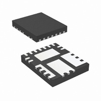
IC REG SYNC BUCK 3A 15-QFN
Manufacturer
International Rectifier
Series
SupIRBuck™r
Type
Step-Down (Buck)r
Datasheet
1.IR3843AMTR1PBF.pdf
(33 pages)
Specifications of IR3843AMTR1PBF
Internal Switch(s)
Yes
Synchronous Rectifier
Yes
Number Of Outputs
1
Voltage - Output
0.7 ~ 18.9 V
Current - Output
3A
Frequency - Switching
225kHz ~ 1.32MHz
Voltage - Input
1.5 ~ 21 V
Operating Temperature
-40°C ~ 125°C
Mounting Type
Surface Mount
Package / Case
15-PowerVQFN
Power - Output
682mW
Part Status
Active
Package
PQFN / 5 x 6
Circuit
Single Output
Iout (a)
3
Switch Freq (khz)
250 - 1200
Input Range (v)
1.5 - 21
Output Range (v)
0.7 - 0.9*Vin
Ocp Otp Uvlo Pre-bias Soft Start And
PGOOD + EN + SEQ
Digital Home Media
Yes
Lead Free Status / RoHS Status
Lead free / RoHS Compliant
Other names
IR3843AMTR1PBFTR


Thermal Shutdown
Temperature
IR3843A. The trip threshold is typically set to
140
shutdown
discharges the soft start capacitor.
Automatic restart is initiated when the sensed
temperature drops within the operating range.
There is a 20
shutdown threshold.
Output Voltage Sequencing
The
programmable sequencing using Seq, Enable
and Power Good pins.
Fig. 8a. Simultaneous Power-up of the slave
Rev 13.0
Through these pins, voltage sequencing such as
simultaneous
implemented. Figure 8. shows simultaneous
sequencing
power-up, the voltage at the Seq pin of the slave
reaches 0.7V before the Fb pin of the master. For
R
the slave follows that of the master until the
voltage at the Seq pin of the slave reaches 0.7 V.
After the voltage at the Seq pin of the slave
exceeds 0.85V, the internal 0.7V reference of
the slave dictates its output voltage.
It is recommended that irrespective of the
sequencing configuration used, the input voltage
should be allowed to come up to its nominal
value first, followed by V
sequencing signal is applied.
For non-sequenced operation, the Seq pin
should be tied to a voltage greater than 0.85V,
such as 3.3V or V
should be allowed to come up before V
Enable.
o
E
C. When trip threshold is exceeded, thermal
/R
F
IR3843A
with respect to the master.
=R
turns
C
/R
Simultaneous Powerup
D
sensing
configurations.
o
, therefore, the output voltage of
C hysteresis in the thermal
and
can
off
cc
. Again, the input voltage
both
cc
is
accommodate
sequential
Vo1
Vo2
and Enable, before the
provided
MOSFETs
In
simultaneous
can
inside
user
cc
and
and
be
RE
RF
1.5V <Vin<16V
Vo(master)
PGood
4.5V <Vcc<5.5V
1.5V <Vin<16V
4.5V <Vcc<5.5V
Power Good Output
The IC continually monitors the output voltage via
Feedback (Fb pin). The feedback voltage forms
an input to a window comparator whose upper
and lower thresholds are 0.805V and 0.595V
respectively. Hence, the Power Good signal is
flagged when the Fb pin voltage is within the
PGood window, i. e., between 0.595V to 0.805V,
as shown in Fig .9 The PGood pin is open drain
and it needs to be externally pulled high. High
state indicates that output is in regulation. Fig. 9a
shows the PGood timing diagram for non-
tracking operation. In this case, during startup,
PGood goes high after the SS voltage reaches
2.1V if the Fb voltage is within the PGood
comparator window. Fig. 9a. and Fig 9.b. also
show a 256 cycle delay between the Fb voltage
entering within the thresholds defined by the
PGood window and PGood going high.
PGood
Fig. 8b. Application Circuit for Simultaneous
Seq
Vcc
Rt
SS/ SD
PGood
Seq
Vcc
Rt
SS/ SD
PGood
Sequencing
Enable
Gnd
Enable
Gnd
IR3843AMPbF
Vin
PGnd
Vin
PGnd
OCSet
Comp
Boot
OCSet
SW
Comp
Fb
Boot
SW
Fb
PD-97509
RA
RC
RB
RD
15
Vo(master)
Vo(slave)
Related parts for IR3843AMTR1PBF
Image
Part Number
Description
Manufacturer
Datasheet
Request
R

Part Number:
Description:
SCHOTTKY RECTIFIER
Manufacturer:
International Rectifier Corp.
Datasheet:
Part Number:
Description:
SCHOTTKY RECTIFIER
Manufacturer:
International Rectifier Corp.
Datasheet:
Part Number:
Description:
SCHOTTKY RECTIFIER
Manufacturer:
International Rectifier Corp.
Datasheet:
Part Number:
Description:
SCHOTTKY RECTIFIER
Manufacturer:
International Rectifier Corp.
Datasheet:
Part Number:
Description:
SCHOTTKY RECTIFIER
Manufacturer:
International Rectifier Corp.
Datasheet:
Part Number:
Description:
SCHOTTKY RECTIFIER
Manufacturer:
International Rectifier Corp.
Datasheet:
Part Number:
Description:
SCHOTTKY RECTIFIER
Manufacturer:
International Rectifier Corp.
Datasheet:
Part Number:
Description:
SCHOTTKY RECTIFIER
Manufacturer:
International Rectifier Corp.
Datasheet:
Part Number:
Description:
SCHOTTKY RECTIFIER
Manufacturer:
International Rectifier Corp.
Datasheet:
Part Number:
Description:
SCHOTTKY RECTIFIER
Manufacturer:
International Rectifier Corp.
Datasheet:
Part Number:
Description:
SCHOTTKY RECTIFIER
Manufacturer:
International Rectifier Corp.
Datasheet:
Part Number:
Description:
SCHOTTKY RECTIFIER
Manufacturer:
International Rectifier Corp.
Datasheet:
Part Number:
Description:
SCHOTTKY RECTIFIER
Manufacturer:
International Rectifier Corp.
Datasheet:
Part Number:
Description:
SCHOTTKY RECTIFIER
Manufacturer:
International Rectifier Corp.
Datasheet:
Part Number:
Description:
SCHOTTKY RECTIFIER
Manufacturer:
International Rectifier Corp.
Datasheet: