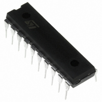
L4972A STMicroelectronics, L4972A Datasheet - Page 4

L4972A
Manufacturer Part Number
L4972A
Description
IC REG SW 2A 5.1V-40V 20-DIP
Manufacturer
STMicroelectronics
Type
Step-Down (Buck)r
Datasheet
1.L4972AD013TR.pdf
(22 pages)
Specifications of L4972A
Internal Switch(s)
Yes
Synchronous Rectifier
No
Number Of Outputs
1
Voltage - Output
5.1 ~ 40 V
Current - Output
2A
Frequency - Switching
100kHz
Voltage - Input
15 ~ 50 V
Operating Temperature
-40°C ~ 150°C
Mounting Type
Through Hole
Package / Case
20-DIP (0.300", 7.62mm)
Power - Output
5W
Output Voltage
50 V
Mounting Style
Through Hole
Input Voltage
50V
Output Current
2A
No. Of Outputs
1
Power Dissipation Pd
5W
No. Of Pins
20
Operating Temperature Range
-40°C To +150°C
Filter Terminals
Through Hole
Rohs Compliant
Yes
Lead Free Status / RoHS Status
Lead free / RoHS Compliant
Other names
497-6698-5
L4972A
L4972A
Available stocks
Company
Part Number
Manufacturer
Quantity
Price
Part Number:
L4972A
Manufacturer:
ST
Quantity:
20 000
Company:
Part Number:
L4972AD
Manufacturer:
STM
Quantity:
3 697
Part Number:
L4972AD
Manufacturer:
STM
Quantity:
20 000
Company:
Part Number:
L4972AD013TR
Manufacturer:
SII
Quantity:
4 466
Part Number:
L4972AD013TR
Manufacturer:
ST
Quantity:
20 000
L4972A
stage. An error signal is produced by comparing the output voltage with the precise 5.1V ± 2% on chip
reference. This error signal is then compared with the sawtooth oscillator in order to generate frixed fre-
quency pulse width modulated drive for the output stage. A PWM latch is included to eliminate multiple
pulsing within a period even in noisy environments.
The gain and stability of the loop can be adjusted by an external RC network connected to the output of
the error amplifier. A voltage feedforward control has been added to the oscillator, this maintains superior
line regulation over a wide input voltage range. Closing the loop directly gives an output vol-tage of 5.1V,
higher voltages are obtained by inserting a voltage divider.
At turn on, output overcurrents are prevented by the soft start function (fig. 5). The error amplifier is initially
clamped by an external capacitor, Css, and allowed to rise linearly under the charge of an internal constant
current source.
Output overload protection is provided by a current limit circuit. The load current is sensed by a internal
metal resistor connected to a comparator. When the load current exceeds a preset threshold, the output
of the comparator sets a flip flop which turns off the power DMOS. The next clock pulse, from an internal
40kHz oscillator, will reset the flip flop and the power DMOS will again conduct. This current protection
method, ensures a constant current output when the system is overloaded or short circuited and limits the
switching frequency, in this condition, to 40kHz. The Reset and Power fail diagram (fig. 7), generates an
output signal when the supply voltage exceeds a threshold programmed by an external voltage divider.
The reset signal, is generated with a delay time programmed by a external capacitor on the delay pin.
When the supply voltage falls below the threshold or the output voltage goes below 5V, the reset output
goes low immediately. The reset output is an open drain.
Fig. 7A shows the case when the supply voltage is higher than the threshold, but the output voltage is not
yet 5V.
Fig. 7B shows the case when the output is 5.1V, but the supply voltage is not yet higher than the fixed
threshold. The thermal protection disables circuit operation when the junction temperature reaches about
150°C and has a hysterysis to prevent unstable conditions.
Figure 4. Feedforward Waveform.
Figure 5. Soft Start Function.
4/22


