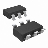
LM2736YMK/NOPB National Semiconductor, LM2736YMK/NOPB Datasheet - Page 3

LM2736YMK/NOPB
Manufacturer Part Number
LM2736YMK/NOPB
Description
IC REG PWM STPDWN 750MA TSOT23-6
Manufacturer
National Semiconductor
Type
Step-Down (Buck)r
Datasheet
1.LM2736YMKNOPB.pdf
(22 pages)
Specifications of LM2736YMK/NOPB
Internal Switch(s)
Yes
Synchronous Rectifier
No
Number Of Outputs
1
Voltage - Output
1.25 ~ 16 V
Current - Output
750mA
Frequency - Switching
550kHz
Voltage - Input
3 ~ 18 V
Operating Temperature
-40°C ~ 125°C
Mounting Type
Surface Mount
Package / Case
TSOT-23-6, TSOT-6
For Use With
LM2736Y EVAL - BOARD EVALUATION LM2736Y
Lead Free Status / RoHS Status
Lead free / RoHS Compliant
Power - Output
-
Other names
LM2736YMK
LM2736YMKTR
LM2736YMKTR
Available stocks
Company
Part Number
Manufacturer
Quantity
Price
Company:
Part Number:
LM2736YMK/NOPB
Manufacturer:
TI
Quantity:
11 670
∆V
Symbol
R
Absolute Maximum Ratings
If Military/Aerospace specified devices are required,
please contact the National Semiconductor Sales Office/
Distributors for availability and specifications.
Electrical Characteristics
Specifications with standard typeface are for T
ture Range (T
limits are guaranteed by design, test, or statistical analysis.
Note 1: Absolute Maximum Ratings indicate limits beyond which damage to the device may occur. Operating Ratings indicate conditions for which the device is
intended to be functional, but specific performance is not guaranteed. For guaranteed specifications and the test conditions, see Electrical Characteristics.
Note 2: Human body model, 1.5kΩ in series with 100pF.
Note 3: Thermal shutdown will occur if the junction temperature exceeds 165˚C. The maximum power dissipation is a function of T
maximum allowable power dissipation at any ambient temperature is P
board with 2oz. copper on 4 layers in still air. For a 2 layer board using 1 oz. copper in still air, θ
Note 4: Guaranteed to National’s Average Outgoing Quality Level (AOQL).
Note 5: Typicals represent the most likely parametric norm.
V
I
UVLO
V
SW Voltage
Boost Voltage
Boost to SW Voltage
FB Voltage
EN Voltage
Junction Temperature
ESD Susceptibility (Note 2)
Storage Temp. Range
D
BOOST
D
FB
DS(ON)
F
EN_TH
V
I
I
I
I
IN
MAX
I
SW
FB
MIN
CL
EN
SW
FB
Q
/∆V
IN
Feedback Voltage
Feedback Voltage Line
Regulation
Feedback Input Bias Current
Undervoltage Lockout
Undervoltage Lockout
UVLO Hysteresis
Switching Frequency
Maximum Duty Cycle
Minimum Duty Cycle
Switch ON Resistance
Switch Current Limit
Quiescent Current
Quiescent Current (shutdown)
Boost Pin Current
Shutdown Threshold Voltage
Enable Threshold Voltage
Enable Pin Current
Switch Leakage
J
= -40˚C to 125˚C). V
Parameter
IN
-0.5V to (V
= 5V, V
-65˚C to 150˚C
-0.5V to 6.0V
-0.5V to 3.0V
-0.5V to 22V
-0.5V to 22V
-0.5V to 28V
J
V
Sink/Source
V
V
LM2736X
LM2736Y
LM2736X
LM2736Y
LM2736X
LM2736Y
V
V
Switching
V
LM2736X (50% Duty Cycle)
LM2736Y (50% Duty Cycle)
V
V
Sink/Source
(Note 1)
BOOST
= 25˚C, and those in boldface type apply over the full Operating Tempera-
IN
IN
IN
BOOST
BOOST
EN
EN
EN
IN
= 3V to 18V
Rising
Falling
+ 0.3V)
= 0V
Falling
Rising
150˚C
- V
2kV
- V
- V
D
Conditions
SW
= (T
SW
SW
J(MAX)
= 5V unless otherwise specified. Datasheet min/max specification
= 3V
= 3V
3
– T
Operating Ratings
Soldering Information
V
SW Voltage
Boost Voltage
Boost to SW Voltage
Junction Temperature Range
Thermal Resistance θ
A
)/θ
IN
Infrared/Convection Reflow (15sec)
Wave Soldering Lead Temp. (10sec)
JA
. All numbers apply for packages soldered directly onto a 3” x 3” PC
JA
= 204˚C/W.
(Note 4)
1.225
0.30
0.40
Min
2.0
1.2
1.0
1.8
85
90
JA
(Note 3)
(Note 5)
1.250
0.01
2.74
0.44
0.55
Typ
350
2.3
1.6
1.5
1.5
2.2
0.9
10
92
96
30
10
40
(Note 1)
2
1
J(MAX)
(Note 4)
−40˚C to +125˚C
1.275
Max
2.90
0.62
0.66
250
650
1.9
2.3
2.5
3.3
1.6
0.4
, θ
-0.5V to 18V
-0.5V to 23V
1.6V to 5.5V
JA
www.national.com
3V to 18V
and T
118˚C/W
220˚C
260˚C
A
Units
% / V
MHz
mΩ
. The
mA
mA
nA
nA
nA
nA
%
%
V
V
A
V


