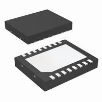
LM3370SD-3416/NOPB National Semiconductor, LM3370SD-3416/NOPB Datasheet - Page 16

LM3370SD-3416/NOPB
Manufacturer Part Number
LM3370SD-3416/NOPB
Description
IC CONV DC/DC DUAL STPDN 16-LLP
Manufacturer
National Semiconductor
Series
PowerWise®r
Type
Step-Down (Buck)r
Datasheet
1.LM3370SD-3021NOPB.pdf
(26 pages)
Specifications of LM3370SD-3416/NOPB
Internal Switch(s)
Yes
Synchronous Rectifier
Yes
Number Of Outputs
2
Voltage - Output
1.4V, 2.8V
Current - Output
600mA
Frequency - Switching
2MHz
Voltage - Input
2.7 ~ 5.5 V
Operating Temperature
-30°C ~ 85°C
Mounting Type
Surface Mount
Package / Case
16-LLP
Power - Output
1.54W
Lead Free Status / RoHS Status
Lead free / RoHS Compliant
Other names
LM3370SD-3416TR
Available stocks
Company
Part Number
Manufacturer
Quantity
Price
Company:
Part Number:
LM3370SD-3416/NOPB
Manufacturer:
National Semiconductor
Quantity:
1 994
www.national.com
F
t
t
t
t
t
t
t
T
T
VDD_I
BF
HOLD
CLKLP
CLKHP
SU
DATAHLD
CLKSU
CLK
SU
TRANS
Symbol
I
Unless otherwise noted, V
appearing in boldface type apply over the entire junction temperature range for operation, −30°C to +125°C. (Notes 2, 8, 9)
I
In I
and the SDA pin is used for the I
need a pull-up resistor according to I
values of the pull-up resistor are determined by the capaci-
tance of the bus (typ.
I
START and STOP bits classify the beginning and the end of
the I
transitioning from HIGH to LOW while SCL line is HIGH.
STOP condition is defined as the SDA transitioning from LOW
to HIGH while SCL is HIGH. The I
2
2
2
C COMPATIBLE START AND STOP CONDITIONS
C Compatible Interface Electrical Specifications
C Compatible Interface
2
C compatible mode, the SCL pin is used for the I
2
2
C
C session. START condition is defined as SDA signal
Clock Frequency
Bus-Free Time between Start and Stop
Hold Time Repeated Start Condition
CLK Low Period
CLK High Period
Set Up Time Repeated Start Condition
Data Hold Time
Data Set Up Time
Set Up Time for Start Condition
Maximum Pulse Width of Spikes that Must be
Suppressed by the Input Filter of Both DATA & CLK
signals.
I
2
C Logic High Level
∼
1.8k). Signal timing specifications are
BATT
= 2.7V to 5.5V. Typical values and limits appearing in normal type apply for T
Parameter
2
2
C master always generates
C data. Both these signals
2
C specification. The
2
C clock
16
according to the I
400 kHz.
I
The data on SDA line must be stable during the HIGH period
of the clock signal (SCL). In other words, state of the data line
can only be changed when CLK is LOW.
START and STOP bits. The I
after START condition and free after STOP condition. During
data transmission, I
conditions. First START and repeated START conditions are
equivalent, function-wise.
Conditions
2
(Note 10)
(Note 10)
(Note 10)
(Note 10)
(Note 10)
(Note 10)
(Note 10)
(Note 10)
(Note 10)
C COMPATIBLE DATA VALIDITY
2
C bus specification. Maximum frequency is
Min
200
200
1.3
0.6
1.3
0.6
0.6
0.6
2
1
C master can generate repeated START
2
C bus is considered to be busy
20167307
Typ
50
20167306
J
= 25°C. Limits
Max
400
V
IN
Units
kHz
µS
µS
µS
µS
µS
nS
nS
µS
nS
V


