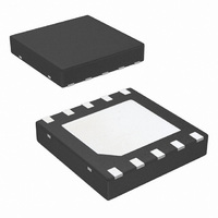
LM25010SD/NOPB National Semiconductor, LM25010SD/NOPB Datasheet - Page 13

LM25010SD/NOPB
Manufacturer Part Number
LM25010SD/NOPB
Description
IC BUCK ADJ 1A 10LLP
Manufacturer
National Semiconductor
Type
Step-Down (Buck)r
Datasheet
1.LM25010SDNOPB.pdf
(18 pages)
Specifications of LM25010SD/NOPB
Internal Switch(s)
Yes
Synchronous Rectifier
No
Number Of Outputs
1
Voltage - Output
2.5 ~ 37 V
Current - Output
1A
Frequency - Switching
100kHz ~ 1MHz
Voltage - Input
6 ~ 42 V
Operating Temperature
-40°C ~ 125°C
Mounting Type
Surface Mount
Package / Case
10-LLP
Primary Input Voltage
42V
No. Of Outputs
1
Output Voltage
37V
Output Current
1A
No. Of Pins
10
Operating Temperature Range
-40°C To +125°C
Msl
MSL 1 - Unlimited
Supply Voltage Range
6V To 42V
Rohs Compliant
Yes
Filter Terminals
SMD
For Use With
LM25010EVAL - BOARD EVALUATION LM25010
Lead Free Status / RoHS Status
Lead free / RoHS Compliant
Power - Output
-
Other names
LM25010SD
LM25010SDTR
LM25010SDTR
Available stocks
Company
Part Number
Manufacturer
Quantity
Price
Company:
Part Number:
LM25010SD/NOPB
Manufacturer:
National Semiconductor
Quantity:
1 894
Part Number:
LM25010SD/NOPB
Manufacturer:
TI/德州仪器
Quantity:
20 000
C3: The capacitor at the VCC pin provides noise filtering and
stability, prevents false triggering of the V
switch on/off transitions, and limits the peak voltage at V
when a high voltage with a short rise time is initially applied
at V
a good quality, low ESR, ceramic capacitor, physically close
to the IC pins.
C4: The recommended value for C4 is 0.022 µF. A high quality
ceramic capacitor with low ESR is recommended as C4 sup-
plies the surge current to charge the buck switch gate at each
turn-on. A low ESR also ensures a complete recharge during
each off-time.
C5: This capacitor suppresses transients and ringing due to
lead inductance at VIN. A low ESR, 0.1 µF ceramic chip ca-
pacitor is recommended, located physically close to the
LM25010.
C6: The capacitor at the SS pin determines the soft-start time,
i.e. the time for the reference voltage at the regulation com-
parator, and the output voltage, to reach their final value. The
capacitor value is determined from the following:
IN
. C3 should be no smaller than 0.47 µF, and should be
CC
UVLO at the buck
FIGURE 6. Example Circuit
CC
13
For a 5 ms softstart time, C6 calculates to 0.022 µF.
D1: A Schottky diode is recommended. Ultra-fast recovery
diodes are not recommended as the high speed transitions at
the SW pin may inadvertently affect the IC’s operation through
external or internal EMI. The diode should be rated for the
maximum V
peak current which occurs when current limit and maximum
ripple current are reached simultaneously (I
previously calculated to be 1.86A. The diode’s forward volt-
age drop affects efficiency due to the power dissipated during
the off-time. The average power dissipation in D1 is calculat-
ed from:
where I
FINAL CIRCUIT
The final circuit is shown in Figure 6, and its performance is
shown in Figures 7 & 8. Current limit measured approximately
1.3A.
O
is the load current, and D is the duty cycle.
IN
(40V), the maximum load current (1A), and the
P
D1
= V
F
x I
O
x (1 - D)
20172733
PK
in Figure 4),
www.national.com


