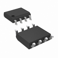
LM2660M/NOPB National Semiconductor, LM2660M/NOPB Datasheet - Page 2

LM2660M/NOPB
Manufacturer Part Number
LM2660M/NOPB
Description
IC MULTI CONFIG .1A 8SOIC
Manufacturer
National Semiconductor
Type
Switched Capacitor (Charge Pump), Divider, Doubler, Invertingr
Datasheet
1.LM2660MM.pdf
(13 pages)
Specifications of LM2660M/NOPB
Internal Switch(s)
Yes
Synchronous Rectifier
No
Number Of Outputs
1
Current - Output
100mA
Frequency - Switching
40kHz
Voltage - Input
1.5 ~ 5.5 V
Operating Temperature
-40°C ~ 85°C
Mounting Type
Surface Mount
Package / Case
8-SOIC (3.9mm Width)
Power - Output
735mW
Primary Input Voltage
5V
No. Of Outputs
1
Output Current
100mA
No. Of Pins
8
Operating Temperature Range
-40°C To +85°C
Msl
MSL 1 - Unlimited
Current Rating
100A
Filter Terminals
SMD
Rohs Compliant
Yes
Lead Free Status / RoHS Status
Lead free / RoHS Compliant
Voltage - Output
-
Other names
*LM2660M
*LM2660M/NOPB
LM2660M
*LM2660M/NOPB
LM2660M
www.national.com
V+
I
I
V
I
R
f
f
I
P
V
Q
SD
L
OSC
SW
OSC
Symbol
SD
OUT
EFF
OEFF
Absolute Maximum Ratings
If Military/Aerospace specified devices are required,
please contact the National Semiconductor Sales Office/
Distributors for availability and specifications.
Electrical Characteristics
Limits in standard typeface are for T
less otherwise specified: V+ = 5V, FC = Open, C
Note 1: Absolute maximum ratings indicate limits beyond which damage to the device may occur. Electrical specifications do not apply when operating the device
beyond its rated operating conditions.
Note 2: OUT may be shorted to GND for one second without damage. However, shorting OUT to V+ may damage the device and should be avoided. Also, for
temperatures above 85˚C, OUT must not be shorted to GND or V+, or device may be damaged.
Note 3: The maximum allowable power dissipation is calculated by using P
ambient temperature, and θ
Note 4: In the test circuit, capacitors C
voltage and efficiency.
Note 5: In doubling mode, when V
Note 6: Specified output resistance includes internal switch resistance and capacitor ESR.
Note 7: For LM2661, the oscillator frequency is 80 kHz.
Note 8: The output switches operate at one half of the oscillator frequency, f
Supply Voltage (V+ to GND, or GND to OUT)
LV
FC, OSC
V+ and OUT Continuous Output Current
Output Short-Circuit Duration to GND (Note
2)
Supply Voltage
Supply Current
Shutdown Supply Current
(LM2661)
Shutdown Pin Input Voltage
(LM2661)
Output Current
Output Resistance (Note 6)
Oscillator Frequency (Note 7)
Switching Frequency (Note 8)
OSC Input Current
Power Efficiency
Voltage Conversion Efficiency
Parameter
JA
is the junction-to-ambient thermal resistance of the specified package.
0.3V) or (V+ − 6V) to (V+ + 0.3V)
out
The least negative of (OUT −
(OUT − 0.3V) to (GND + 3V)
>
1
5V, minimum input high for shutdown equals V
and C
J
2
= 25˚C, and limits in boldface type apply over the full operating temperature range. Un-
are 0.2Ω maximum ESR capacitors. Capacitors with higher ESR will increase output resistance, reduce output
R
No Load
LV = Open
Shutdown Mode
Normal Operation
T
T
I
OSC = Open
OSC = Open
FC = Open
FC = V+
R
R
I
No Load
L
L
(Note 1)
A
A
L
L
L
= 100 mA
= 100 mA to GND
1
= 1k
≤ +85˚C, OUT ≤ −4V
(1k) between V
(500) between GND and OUT
>
= C
120 mA
+85˚C, OUT ≤ −3.8V
1 sec.
2
6V
= 150 µF. (Note 4)
DMax
OSC
2
Condition
= (T
= 2f
Inverter, LV = Open
Inverter, LV = GND
Doubler, LV = OUT
FC = Open (LM2660)
FC = V+ (LM2660) or
SD = Ground (LM2661)
T
T
FC = Open
FC = V+
FC = Open
FC = V+
+
A
A
and OUT
JMax
SW
Power Dissipation
T
θ
Operating Junction
Temperature
Storage Temperature
Range
Lead Temperature
ESD Rating
≤ +85˚C
>
JA
out
J
.
(T
Range
(Soldering, 10 seconds)
+85˚C
Max (Note 3)
− T
− 3V.
(Note 3)
A
A
= 25˚C) (Note 3)
)/θ
JA
, where T
JMax
is the maximum junction temperature, T
Min
100
100
3.5
1.5
2.5
2.0
2.5
40
20
96
92
99
5
170˚C/W
735 mW
150˚C
(Note 5)
M
99.96
0.12
Typ
±
0.5
6.5
10
80
40
±
98
96
88
1
5
16
2
Package
−65˚C to +150˚C
−40˚C to +85˚C
250˚C/W
Max
500 mW
5.5
5.5
5.5
0.5
0.3
10
12
150˚C
3
2
MM
300˚C
A
2 kV
is the
Units
kHz
kHz
mA
mA
µA
µA
%
%
Ω
V
V


