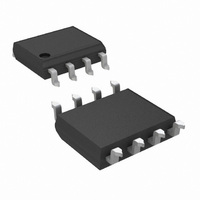
LM2578AM/NOPB National Semiconductor, LM2578AM/NOPB Datasheet - Page 14

LM2578AM/NOPB
Manufacturer Part Number
LM2578AM/NOPB
Description
IC REG SIMPLE SWITCHER 8-SOIC
Manufacturer
National Semiconductor
Type
Step-Down (Buck), Step-Up (Boost), Inverting, Flybackr
Datasheet
1.LM3578AMNOPB.pdf
(20 pages)
Specifications of LM2578AM/NOPB
Internal Switch(s)
Yes
Synchronous Rectifier
No
Number Of Outputs
1
Current - Output
750mA
Frequency - Switching
20kHz
Voltage - Input
2 ~ 40 V
Operating Temperature
-40°C ~ 85°C
Mounting Type
Surface Mount
Package / Case
8-SOIC (3.9mm Width)
Primary Input Voltage
40V
No. Of Outputs
1
Output Current
750mA
No. Of Pins
8
Operating Temperature Range
-40°C To +85°C
Msl
MSL 1 - Unlimited
Input Voltage Primary Max
40V
Rohs Compliant
Yes
Lead Free Status / RoHS Status
Lead free / RoHS Compliant
Voltage - Output
-
Power - Output
-
Other names
*LM2578AM
*LM2578AM/NOPB
LM2578AM
*LM2578AM/NOPB
LM2578AM
www.national.com
Typical Applications
Step 1: Calculate the maximum DC current through the
inductor, I
the top of the chart and show that I
buck configuration. Thus, I
Step 2: Calculate the inductor Volts-sec product, E-T
according to the equations given from the chart. For the
Buck:
E-T
=(15 − 5) (5/15) (1000/50)
= 66V-µs.
with the oscillator frequency, f
Step 3: Using the graph with axis labeled “Discontinuous At
% I
maximum inductor current, I
discontinuity percentage.
In this example, the point of interest is where the 0.35A line
intersects with the 20% line. This is nearly the midpoint of the
horizontal axis.
Step 4: This last step is merely the translation of the point
found in Step 3 to the graph directly below it. This is accom-
plished by moving straight down the page to the point which
intercepts the desired E-T
66V-µs and the desired inductor value is 470 µH. Since this
example was for 20% discontinuity, the bottom chart could
have been used directly, as noted in step 3 of the chart
instructions.
For a full line of standard inductor values, contact Pulse
Engineering (San Diego, Calif.) regarding their PE526XX
series, or A. I. E. Magnetics (Nashville, Tenn.).
A more precise inductance value may be calculated for the
Buck, Boost and Inverting Regulators as follows:
BUCK
L = V
BOOST
L = V
INVERT
L = V
where ∆I
usually chosen based on the minimum load current expected
of the circuit. For the buck regulator, since the inductor
current I
op
OUT
o
in
in
= (V
(V
” and “I
(V
|V
L
L
in
o
o
L(max)
equals the load current I
in
|/[∆I
is the current ripple through the inductor. ∆I
− V
− V
− V
L
L(max, DC)
o
in
. The necessary equations are indicated at
(V
)/(∆I
o
)/(∆I
) (V
in
+ |V
L
L
o
/V
V
f
osc
in
o
in
” find the point where the desired
|)f
) (1000/f
f
osc
V
L(max)
osc
op
o
L(max, DC)
)
)
. For this example, E-T
]
osc
, expressed in kHz.
= 350 mA.
osc
O
,
)
(Continued)
L(max)
intercepts the desired
= I
o(max)
for the
op
L
op
is
is
,
14
∆I
∆I
∆I
where the Discontinuity Factor is the ratio of the minimum
load current to the maximum load current. For this example,
the Discontinuity Factor is 0.2.
The remainder of the components of Figure 15 are chosen
as follows:
C1 is the timing capacitor found in Figure 1.
C2 ≥ V
where V
C3 is necessary for continuous operation and is generally in
the 10 pF to 30 pF range.
D1 should be a Schottky type diode, such as the 1N5818 or
1N5819.
BUCK WITH BOOSTED OUTPUT CURRENT
For applications requiring a large output current, an external
transistor may be used as shown in Figure 17. This circuit
steps a 15V supply down to 5V with 1.5A of output current.
The output ripple is 50 mV, with an efficiency of 80%, a load
regulation of 40 mV (150 mA to 1.5A), and a line regulation
of 20 mV (12V ≤ V
Component values are selected as outlined for the buck
regulator with a discontinuity factor of 10%, with the addition
of R4 and R5:
R4 = 10V
R5 = (V
where:
V
V
tor.
V is the current limit sense voltage.
B
Figure 17 ).
I
I
R4
p
BE1
sat
f
L
L
L
= I
is the forced current gain of transistor Q1 (B
= V
= 2 • I
= 140 mA for this circuit. ∆I
= 2 • (Discontinuity Factor) • I
is the saturation voltage of the LM2578A output transis-
L(max, DC)
is the V
o
BE1
in
ripple
(V
BE1
− V − V
O(min)
/R4
in
B
− V
BE
is the peak-to-peak output voltage ripple.
f
/I
+ 0.5∆I
p
of transistor Q1.
o
)/(8f
BE1
in
≤ 18V).
osc
− V
L
2
sat
V
in
) B
V
ripple
f
L
/(I
can also be interpreted as
L(max, DC)
L
L1)
+ I
R4
)
f
= 30 for


