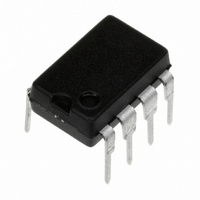
LM2594N-5.0/NOPB National Semiconductor, LM2594N-5.0/NOPB Datasheet - Page 5

LM2594N-5.0/NOPB
Manufacturer Part Number
LM2594N-5.0/NOPB
Description
IC REG SIMPLE SWITCHER 8-DIP
Manufacturer
National Semiconductor
Series
SIMPLE SWITCHER®r
Type
Step-Down (Buck)r
Specifications of LM2594N-5.0/NOPB
Internal Switch(s)
Yes
Synchronous Rectifier
No
Number Of Outputs
1
Voltage - Output
5V
Current - Output
500mA
Frequency - Switching
150kHz
Voltage - Input
4.5 ~ 40 V
Operating Temperature
-40°C ~ 125°C
Mounting Type
Through Hole
Package / Case
8-DIP (0.300", 7.62mm)
Current, Input Bias
10 nA
Current, Output
0.5 A
Current, Supply
5 mA
Frequency, Oscillator
150 kHz
Package Type
DIP-8
Regulator Type
Buck (Step-Down)
Temperature, Operating, Range
-40 to +125 °C
Voltage, Input
4.5 to 40 V
Voltage, Output
5 V
Primary Input Voltage
12V
No. Of Outputs
1
Output Voltage
5V
Output Current
500mA
No. Of Pins
8
Operating Temperature Range
-40°C To +125°C
Peak Reflow Compatible (260 C)
Yes
Rohs Compliant
Yes
Supply Voltage Range
4.5V To 40V
Input Voltage Primary Max
40V
Lead Free Status / RoHS Status
Lead free / RoHS Compliant
Power - Output
-
Lead Free Status / Rohs Status
RoHS Compliant part
Electrostatic Device
Other names
*LM2594N-5.0
*LM2594N-5.0/NOPB
LM2594N-5.0
*LM2594N-5.0/NOPB
LM2594N-5.0
All Output Voltage Versions
Electrical Characteristics
Note 2: The human body model is a 100 pF capacitor discharged through a 1.5k resistor into each pin.
Note 3: Typical numbers are at 25˚C and represent the most likely norm.
Note 4: All limits guaranteed at room temperature (standard type face) and at temperature extremes (bold type face). All room temperature limits are 100% produc-
tion tested. All limits at temperature extremes are guaranteed via correlation using standard Statistical Quality Control (SQC) methods. All limits are used to calculate
Average Outgoing Quality Level (AOQL).
Note 5: External components such as the catch diode, inductor, input and output capacitors, and voltage programming resistors can affect switching regulator sys-
tem performance. When the LM2594/LM2594HV is used as shown in the Figure 1 test circuit, system performance will be as shown in system parameters section
of Electrical Characteristics.
Note 6: The switching frequency is reduced when the second stage current limit is activated. The amount of reduction is determined by the severity of current over-
load.
Note 7: No diode, inductor or capacitor connected to output pin.
Note 8: Feedback pin removed from output and connected to 0V to force the output transistor switch ON.
Note 9: Feedback pin removed from output and connected to 12V for the 3.3V, 5V, and the ADJ. version, and 15V for the 12V version, to force the output transistor
switch OFF.
Note 10: V
Note 11: Junction to ambient thermal resistance with approximately 1 square inch of printed circuit board copper surrounding the leads. Additional copper area will
lower thermal resistance further. See application hints in this data sheet and the thermal model in Switchers Made Simple
Typical Performance Characteristics
Normalized
Output Voltage
Switch Saturation
Voltage
IN
= 40V for the LM2594 and 60V for the LM2594HV.
DS012439-7
DS012439-4
(Continued)
Line Regulation
Switch Current Limit
5
DS012439-8
DS012439-5
Efficiency
Dropout Voltage
®
software.
www.national.com
DS012439-6
DS012439-9


