LM20134MH/NOPB National Semiconductor, LM20134MH/NOPB Datasheet - Page 2
LM20134MH/NOPB
Manufacturer Part Number
LM20134MH/NOPB
Description
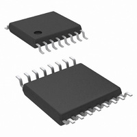
IC BUCK SYNC ADJ 4A 16TSSOP
Manufacturer
National Semiconductor
Series
PowerWise®r
Type
Step-Down (Buck)r
Datasheet
1.LM20134MHNOPB.pdf
(22 pages)
Specifications of LM20134MH/NOPB
Internal Switch(s)
Yes
Synchronous Rectifier
Yes
Number Of Outputs
1
Voltage - Output
0.8 ~ 5 V
Current - Output
4A
Frequency - Switching
410kHz
Voltage - Input
2.95 ~ 5.5 V
Operating Temperature
-40°C ~ 125°C
Mounting Type
Surface Mount
Package / Case
16-TSSOP Exposed Pad, 16-eTSSOP, 16-HTSSOP
Power - Output
2.6W
For Use With
LM20134EVAL - BOARD EVAL 4A POWERWISE LM20134
Lead Free Status / RoHS Status
Lead free / RoHS Compliant
Other names
*LM20134MH/NOPB
LM20134MH
LM20134MH
Available stocks
Company
Part Number
Manufacturer
Quantity
Price
Company:

Part Number:
LM20134MH/NOPB
Manufacturer:
MICREL
Quantity:
1 001


www.national.com
Connection Diagram
Ordering Information
Pin Descriptions
Order Number
LM20134MHE
LM20134MHX
10,11
Pin #
LM20134MH
6,7
8,9
EP
12
13
14
15
16
1
2
3
4
5
Exposed Pad
PGOOD
SS/TRK
COMP
PGND
AGND
Name
SYNC
PVIN
AVIN
VCC
SW
NC
EN
FB
Package Type
eTSSOP-16
Soft-Start or Tracking control input. An internal 5 µA current source charges an external capacitor to
set the Soft-Start ramp rate. If driven by a external source less tan 800 mV, this pin overrides the
internal reference that sets the output voltage. If left open, an internal 1ms Soft-Start ramp is activated.
Feedback input to the error amplifier from the regulated output. This pin is connected to the inverting
input of the internal transconductance error amplifier. An 800 mV reference connected to the non-
inverting input of the error amplifier sets the closed loop regulation voltage at the FB pin.
Power good output signal. Open drain output indicating the output voltage is regulating within
tolerance. A pull-up resistor of 10 to 100 kΩ is recommend for most applications.
External compensation pin. Connect a resistor and capacitor to this pin to compensate the device.
These pins must be connected to GND to ensure proper operation.
Input voltage to the power switches inside the device. These pins should be connected together at the
device. A low ESR capacitor should be placed near these pins to stabilize the input voltage.
Switch pin. The PWM output of the internal power switches.
Power ground pin for the internal power switches.
Precision enable input for the device. An external voltage divider can be used to set the device turn-
on threshold. If not used the EN pin should be connected to PVIN.
Internal 2.7V sub-regulator. This pin should be bypassed with a 1 µF ceramic capacitor.
Analog input supply that generates the internal bias. Must be connected to VIN through a low pass
RC filter.
Quiet analog ground for the internal bias circuitry.
Frequency synchronization pin. An external clock connected to this pin will set the switching frequency.
If left open the device will operate at approximately 410 kHz.
Exposed metal pad on the underside of the package with a weak electrical connection to ground. It is
recommended to connect this pad to the PC board ground plane in order to improve heat dissipation.
NSC Package Drawing
eTSSOP-16 Package
MXA16A
Top View
2
Description
Package Marking
30030402
20134MH
2500 Units of Tape and Reel
250 Units of Tape and Reel
92 Units of Rail
Supplied As
Related parts for LM20134MH/NOPB
Image
Part Number
Description
Manufacturer
Datasheet
Request
R

Part Number:
Description:
Manufacturer:
National Semiconductor
Datasheet:
Part Number:
Description:
National Semiconductor [8-Bit D/A Converter]
Manufacturer:
National Semiconductor
Datasheet:
Part Number:
Description:
National Semiconductor [Media Coprocessor]
Manufacturer:
National Semiconductor
Datasheet:
Part Number:
Description:
Digitally Controlled Tone and Volume Circuit with Stereo Audio Power Amplifier, Microphone Preamp Stage and National 3D Sound
Manufacturer:
National Semiconductor
Datasheet:
Part Number:
Description:
Digitally Controlled Tone and Volume Circuit with Stereo Audio Power Amplifier, Microphone Preamp Stage and National 3D Sound
Manufacturer:
National Semiconductor
Datasheet:
Part Number:
Description:
AC97 Rev 2 Codec with Sample Rate Conversion and National 3D Sound
Manufacturer:
National Semiconductor
Part Number:
Description:
Manufacturer:
National Semiconductor
Datasheet:
Part Number:
Description:
Manufacturer:
National Semiconductor
Datasheet:
Part Number:
Description:
General Purpose, Low Voltage, Low Power, Rail-to-Rail Output Operational Amplifiers
Manufacturer:
National Semiconductor
Datasheet:
Part Number:
Description:
8-bit 20 MSPS flash A/D converter.
Manufacturer:
National Semiconductor
Datasheet:
Part Number:
Description:
Low Noise Quad Operational Amplifier
Manufacturer:
National Semiconductor
Datasheet:
Part Number:
Description:
Quad Differential Line Receivers
Manufacturer:
National Semiconductor
Datasheet:
Part Number:
Description:
Quad High Speed Trapezoidal? Bus Transceiver
Manufacturer:
National Semiconductor
Datasheet:
Part Number:
Description:
Dual Line Receiver
Manufacturer:
National Semiconductor
Datasheet: