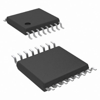
LM2854MH-1000/NOPB National Semiconductor, LM2854MH-1000/NOPB Datasheet - Page 18

LM2854MH-1000/NOPB
Manufacturer Part Number
LM2854MH-1000/NOPB
Description
IC REG 4A SYNC SMPL SW 16ETSSOP
Manufacturer
National Semiconductor
Series
PowerWise®, SIMPLE SWITCHER®r
Type
Step-Down (Buck)r
Datasheet
1.LM2854MH-1000NOPB.pdf
(22 pages)
Specifications of LM2854MH-1000/NOPB
Internal Switch(s)
Yes
Synchronous Rectifier
Yes
Number Of Outputs
1
Voltage - Output
0.8 ~ 5 V
Current - Output
4A
Frequency - Switching
1MHz
Voltage - Input
2.95 ~ 5.5 V
Operating Temperature
-40°C ~ 125°C
Mounting Type
Surface Mount
Package / Case
16-TSSOP Exposed Pad, 16-eTSSOP, 16-HTSSOP
Primary Input Voltage
5.5V
No. Of Outputs
1
Output Voltage
5V
Output Current
4A
Voltage Regulator Case Style
TSSOP
No. Of Pins
16
Operating Temperature Range
-40°C To +125°C
Svhc
No SVHC (15-Dec-2010)
Rohs Compliant
Yes
Lead Free Status / RoHS Status
Lead free / RoHS Compliant
Power - Output
-
Other names
*LM2854MH-1000
*LM2854MH-1000/NOPB
LM2854MH-1000
*LM2854MH-1000/NOPB
LM2854MH-1000
Available stocks
Company
Part Number
Manufacturer
Quantity
Price
Company:
Part Number:
LM2854MH-1000/NOPB
Manufacturer:
MAXIM
Quantity:
5
www.national.com
PC Board Layout Guidelines
PC board layout is an important part of DC-DC converter de-
sign. Poor board layout can disrupt the performance of a DC-
DC converter and surrounding circuitry by contributing to EMI,
ground bounce and resistive voltage drop in the traces. These
can send erroneous signals to the DC-DC converter resulting
in poor regulation or instability. Good layout can be imple-
mented by following a few simple design rules.
1. Minimize area of switched current loops.
There are two loops where currents are switched at high di/
dt slew rates in a buck regulator. The first loop represents the
path taken by AC current flowing during the high side PFET
on time. This current flows from the input capacitor to the reg-
ulator PVIN pins, through the high side FET to the regulator
SW pin, filter inductor, output capacitor and returning via the
PCB ground plane to the input capacitor.
The second loop represents the path taken by AC current
flowing during the low side NFET on time. This current flows
from the output capacitor ground to the regulator PGND pins,
through the NFET to the inductor and output capacitor. From
an EMI reduction standpoint, it is imperative to minimize this
loop area during PC board layout by physically locating the
input capacitor close to the LM2854. Specifically, it is advan-
tageous to place C
and PGND pins. Grounding for both the input and output ca-
pacitor should consist of a localized top side plane that con-
nects to PGND and the exposed die attach pad (DAP). The
inductor should be placed close to the SW pin and output ca-
pacitor.
IN
as close as possible to the LM2854 PVIN
30052853
18
2. Minimize the copper area of the switch node.
The LM2854 has two SW pins optimally located on one side
of the package. In general the SW pins should be connected
to the filter inductor on the top PCB layer. The inductor should
be placed close to the SW pins to minimize the copper area
of the switch node.
3. Have a single point ground for all device analog
grounds located under the DAP.
The ground connections for the Feedback, Soft-start, Enable
and AVIN components should be routed to the AGND pin of
the device. The AGND pin should connect to PGND under the
DAP. This prevents any switched or load currents from flow-
ing in the analog ground traces. If not properly handled, poor
grounding can result in degraded load regulation or erratic
switching behavior.
4. Minimize trace length to the FB pin.
Since the feedback (FB) node is high impedance, the trace
from the output voltage setpoint resistor divider to FB pin
should be as short as possible. This is most important as rel-
atively high value resistors are used to set the output voltage.
The FB trace should be routed away from the SW pin and
inductor to avoid noise pickup from the SW pin. Both feedback
resistors, R
R
5. Make input and output bus connections as wide as
possible.
This reduces any voltage drops on the input or output of the
converter and maximizes efficiency. To optimize voltage ac-
curacy at the load, ensure that a separate feedback voltage
sense trace is made to the load. Doing so will correct for volt-
age drops and provide optimum output accuracy.
6. Provide adequate device heat-sinking.
Use an array of heat-sinking vias to connect the DAP to the
ground plane on the bottom PCB layer. If the PCB has a plu-
rality of copper layers, these thermal vias can also be em-
ployed to make connection to inner layer heat-spreading
ground planes. For best results use a 5 x 3 via array with
minimum via diameter of 10 mils. Ensure enough copper area
is used to keep the junction temperature below 125°C.
COMP
and C
FB1
COMP
and R
, should be located close to the FB pin.
FB2
, and the compensation components,


