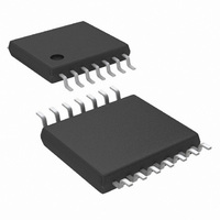
LM5010AQ0MH/NOPB National Semiconductor, LM5010AQ0MH/NOPB Datasheet - Page 12

LM5010AQ0MH/NOPB
Manufacturer Part Number
LM5010AQ0MH/NOPB
Description
IC REG SW 1A SD 14TSSOP AUTO
Manufacturer
National Semiconductor
Type
Step-Down (Buck)r
Datasheet
1.LM5010AMHNOPB.pdf
(18 pages)
Specifications of LM5010AQ0MH/NOPB
Internal Switch(s)
Yes
Synchronous Rectifier
No
Number Of Outputs
1
Voltage - Output
2.5 ~ 70 V
Current - Output
1A
Frequency - Switching
1MHz
Voltage - Input
6 ~ 75 V
Operating Temperature
-40°C ~ 150°C
Mounting Type
Surface Mount
Package / Case
14-TSSOP Exposed Pad, 14-eTSSOP 14-HTSSOP
Package
14TSSOP EP
Minimum Input Voltage
6 V
Maximum Input Voltage
75 V
Switching Frequency
50 to 1000 KHz
Operating Supply Voltage
6 to 75 V
Maximum Output Current
1 A
Output Type
Adjustable
Output Voltage
2.5 to 70 V
Efficiency
91 %
Lead Free Status / RoHS Status
Lead free / RoHS Compliant
Power - Output
-
Other names
*LM5010AQ0MH/NOPB
LM5010AQ0MH
LM5010AQ0MH
www.national.com
To keep the circuit in continuous conduction mode, the max-
imum allowed ripple current is twice the minimum load cur-
rent, or 400 mAp-p. Using this value of ripple current, the
inductor (L1) is calculated using the following:
where F
- 25%) at V
This provides a minimum value for L1 - the next higher stan-
dard value (100 µH) will be used. To prevent saturation, and
possible destructive current levels, L1 must be rated for the
peak current which occurs if the current limit and maximum
ripple current are reached simultaneously (I
The maximum ripple amplitude is calculated by re-arranging
Equation 11 using V
value, based on the manufacturer’s tolerance. Assume, for
this exercise, the inductor’s tolerance is ±20%.
where I
At the nominal maximum load current of 1.0A, the peak in-
ductor current is 1.186A.
R
current waveform does not exceed 1.0A at maximum load
current (see Figure 5), it is not necessary to increase the cur-
rent limit threshold. Therefore R
exercise. For applications where the lower peak exceeds
1.0A, see the section entitled Increasing The Current Limit
Threshold.
C1: This capacitor limits the ripple voltage at VIN resulting
from the source impedance of the supply feeding this circuit,
and the on/off nature of the switch current into VIN. At maxi-
mum load current, when the buck switch turns on, the current
into VIN steps up from zero to the lower peak of the inductor
current waveform (I
CL
: Since it is obvious that the lower peak of the inductor
LIM
I
S(min)
PK
is the maximum guaranteed current limit threshold.
= I
IN(max)
LIM
is the minimum frequency of 154 kHz (205 kHz
+ I
.
OR(max)
PK-
IN(max)
in Figure 5), ramps up to the peak val-
, F
= 1.5A + 0.372A = 1.872A
S(min)
, and the minimum inductor
CL
is not needed for this
PK
in Figure 4).
FIGURE 5. Inductor Current
(11)
(12)
12
ue (I
into VIN during this on-time is the load current. For a worst
case calculation, C1 must supply this average current during
the maximum on-time. The maximum on-time is calculated at
V
The voltage at VIN should not be allowed to drop below 5.5V
in order to maintain V
Normally a lower value can be used for C1 since the above
calculation is a worst case calculation which assumes the
power source has a high source impedance. A quality ceramic
capacitor with a low ESR should be used for C1.
C2 and R3: Since the LM5010A requires a minimum of 25
mVp-p of ripple at the FB pin for proper operation, the required
ripple at V
This necessary ripple voltage is created by the inductor ripple
current acting on C2’s ESR + R3. First, the minimum ripple
current, which occurs at minimum VIN, maximum inductor
value, and maximum frequency, is determined.
The minimum ESR for C2 is then equal to:
If the capacitor used for C2 does not have sufficient ESR, R3
is added in series as shown in the Block Diagram. The value
chosen for C2 is application dependent, and it is recommend-
ed that it be no smaller than 3.3 µF. C2 affects the ripple at
V
essary to determine the optimum value for C2.
IN
OUT
= 6V using Equation 5, with a 25% tolerance added:
PK+
, and transient response. Experimentation is usually nec-
V
), then drops to zero at turn-off. The average current
RIPPLE
OUT
= 25 mVp-p x (R1 + R2)/R2 = 50 mVp-p
is increased by R1 and R2, and is equal to:
CC
above its UVLO.
20153822
(13)


