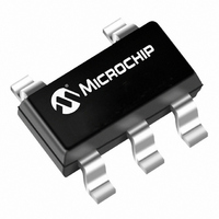
TCM828ECT713 Microchip Technology, TCM828ECT713 Datasheet - Page 15

TCM828ECT713
Manufacturer Part Number
TCM828ECT713
Description
IC CHARGE PUMP CONV SOT23A-5
Manufacturer
Microchip Technology
Type
Switched Capacitor (Charge Pump), Doubler, Invertingr
Specifications of TCM828ECT713
Package / Case
SOT-23-5, SC-74A, SOT-25
Internal Switch(s)
Yes
Synchronous Rectifier
No
Number Of Outputs
1
Voltage - Output
-1.5 ~ -5.5 V, ±3 ~ ±11 V
Current - Output
25mA
Frequency - Switching
12kHz
Voltage - Input
1.5 ~ 5.5 V
Operating Temperature
-40°C ~ 85°C
Mounting Type
Surface Mount
Power - Output
240mW
Minimum Operating Temperature
- 40 C
Mounting Style
SMD/SMT
Function
Inverting, Step Up
Output Voltage
- 1.5 V to - 5.5 V, 3 V to 11 V
Output Current
25 mA
Maximum Operating Temperature
85 C
Lead Free Status / RoHS Status
Lead free / RoHS Compliant
Lead Free Status / RoHS Status
Lead free / RoHS Compliant, Lead free / RoHS Compliant
Other names
158-2031-2
158-2031-2
TCM828ECT713TR
158-2031-2
TCM828ECT713TR
Available stocks
Company
Part Number
Manufacturer
Quantity
Price
Company:
Part Number:
TCM828ECT713
Manufacturer:
MICROCHIP
Quantity:
12 000
Part Number:
TCM828ECT713
Manufacturer:
MICROCHIP/微芯
Quantity:
20 000
5.0.7
To reduce the value of R
TCM829 devices can be connected in parallel
(Figure
a factor of N, where N is the number of TCM828/
TCM829 device. Each device will require it’s own pump
capacitor (C1), but all devices may share one reservoir
capacitor
performance, the value of C2 should be scaled
according to the number of paralleled TCM828/
TCM829 devices.
FIGURE 5-5:
TCM829 Devices to Reduce Output Resistance.
5.0.8
Another common application of the TCM828/TCM829
devices is shown in
two functions in combination. C1 and C2 form the
standard inverter circuit described above. C3 and C4,
plus the two diodes, form the voltage doubler circuit. C1
and C3 are the pump capacitors, while C2 and C4 are
the reservoir capacitors. Because both sub-circuits rely
on the same switches, if either output is loaded, both
will drop toward GND. Make sure that the total current
drawn from both the outputs does not total more than
40 mA.
© 2010 Microchip Technology Inc.
C1
5-5). The output resistance will be reduced by
3
4
5
PARALLELING DEVICES
VOLTAGE DOUBLER/INVERTER
(C2).
TCM828/
TCM829
"1"
However,
R
Figure
OUT
V
2
Paralleling TCM828 or
1
C1
+
IN
=
V
NUMBER OF DEVICES
5-6. This circuit performs
OUT
. . .
OUT
. . .
3
4
5
to
V
OF SINGLE DEVICE
, multiple TCM828/
OUT
TCM828/
TCM829
preserve
"n"
= V
-
IN
1
2
C2
V
ripple
OUT
FIGURE 5-6:
Inverter.
5.0.9
When heavy loads require the OUT pin to sink large
currents, being delivered by a positive source, diode
protection may be needed. The OUT pin should not be
allowed to be pulled above ground. This is
accomplished by connecting a Schottky diode
(1N5817) as shown in
FIGURE 5-7:
5.0.10
As with any switching power supply circuit, good layout
practice is recommended. Mount components as close
together as possible, to minimize stray inductance and
capacitance. Also use a large ground plane to minimize
noise leakage into other circuitry.
C1
3
4
5
TCM828/TCM829
DIODE PROTECTION FOR HEAVY
LOADS
LAYOUT CONSIDERATIONS
TCM828/
TCM829
C3
TCM828/
TCM829
Combined Doubler and
Figure
High V
2
1
GND
V
OUT
+
IN
5-7.
–
4
1
D1
D2
Load Current.
D1, D2 = 1N4148
DS21488B-page 15
C2
C4
V
(V
V
OUT
OUT
FD1
) - (V
= (2V
= V
-
IN
FD2
IN
) -
)


