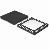
MAX8686ETL+ Maxim Integrated Products, MAX8686ETL+ Datasheet - Page 22

MAX8686ETL+
Manufacturer Part Number
MAX8686ETL+
Description
IC BUCK SYNC ADJ 25A 40TQFN
Manufacturer
Maxim Integrated Products
Type
Step-Down (Buck)r
Datasheet
1.MAX8686ETL.pdf
(23 pages)
Specifications of MAX8686ETL+
Internal Switch(s)
Yes
Synchronous Rectifier
Yes
Number Of Outputs
1
Voltage - Output
0.7 ~ 5.5 V
Current - Output
25A
Frequency - Switching
300kHz ~ 1MHz
Voltage - Input
4.5 ~ 20 V
Operating Temperature
-40°C ~ 85°C
Mounting Type
Surface Mount
Package / Case
40-TQFN Exposed Pad
Power - Output
4W
Lead Free Status / RoHS Status
Lead free / RoHS Compliant
Single/Multiphase, Step-Down,
DC-DC Converter Delivers Up to 25A Per Phase
Careful PCB layout is critical to achieve low switching
losses and clean, stable operation. The switching
power stage requires particular attention. Follow these
guidelines for good PCB layout:
1)
2)
3)
22
PHASE/REFO
TOP VIEW
Place IC decoupling capacitors as close to the IC
pins as possible. Separate the power and analog
ground planes. Place the input ceramic decoupling
capacitor directly across and as close as possible
to IN and PGND. This is to help contain the high
switching current within this small loop.
For output current greater than 10A, a four-layer
PCB is recommended. Pour an analog ground
plane in the second layer underneath the IC to min-
imize noise coupling.
Connect input and output capacitor to the PGND
plane and the VL capacitor to RTN. Connect all
analog signals to GND. The frequency-setting
capacitor should be connected to GFREQ.
______________________________________________________________________________________
COMP
REFIN
FREQ
ILIM
POK
BST
RS+
RS-
SS
31
32
33
34
35
36
37
38
39
40
+
30
1
Applications Information
GND_EP
29
2
28
3
27
4
MAX8686
PCB Layout Guidelines
TQFN
26
5
Pin Configuration
25
6
IN_EP
LX_EP
24 23 22
7
8
9
10
21
20 IN
19
18
17
16
15
14
13
12
11
IN
IN
N.C.
LX
PGND
PGND
PGND
PGND
PGND
4)
5)
6)
7)
8)
9)
10) Refer to the MAX8686 Evaluation Kit for an exam-
For the latest package outline information and land patterns, go
to www.maxim-ic.com/packages. Note that a “+”, “#”, or “-” in
the package code indicates RoHS status only. Package draw-
ings may show a different suffix character, but the drawing per-
tains to the package regardless of RoHS status.
PROCESS: BiCMOS
PACKAGE TYPE
Connect PGND, GND, and RTN at the return path
of the input bypass capacitor.
Signals shared by the master and slave (ILIM,
COMP, and FREQ) should not run close to switch-
ing signals.
Place the inductor current-sense resistor and
capacitor as close to the inductor as possible.
Make a Kelvin connection to minimize the effect of
PCB trace resistance.
Connect the exposed pad sections to the corre-
sponding IC pins and allow sufficient copper area
to help cooling the device.
Place the REFIN and compensation components
as close to the IC pins as possible.
Connect remote-sense input RS+ and RS- directly
to the load voltage regulation point and use Kelvin
connection for the two traces.
ple layout.
40 TQFN
40 TQFN
PACKAGE CODE
Package Information
T4066MN+1
T4066M+1
Chip Information
DOCUMENT NO.
21-0177
21-0177


