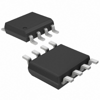
MAX5033CASA+ Maxim Integrated Products, MAX5033CASA+ Datasheet - Page 11

MAX5033CASA+
Manufacturer Part Number
MAX5033CASA+
Description
IC DC-DC CONV HI EFF 8-SOIC
Manufacturer
Maxim Integrated Products
Type
Step-Down (Buck)r
Datasheet
1.MAX5033AUSA.pdf
(17 pages)
Specifications of MAX5033CASA+
Internal Switch(s)
Yes
Synchronous Rectifier
No
Number Of Outputs
1
Voltage - Output
12V
Current - Output
500mA
Frequency - Switching
125kHz
Voltage - Input
7.5 ~ 76 V
Operating Temperature
-40°C ~ 125°C
Mounting Type
Surface Mount
Package / Case
8-SOIC (3.9mm Width)
Power - Output
471mW
Lead Free Status / RoHS Status
Lead free / RoHS Compliant
Ensure that the ripple specification of the input capaci-
tor exceeds the worst-case capacitor RMS ripple cur-
rent. Use the following equations to calculate the input
capacitor RMS current:
I
input average current, and η is the converter efficiency.
The ESR of aluminum electrolytic capacitors increases
significantly at cold temperatures. Use a 1µF or greater
value ceramic capacitor in parallel with the aluminum
electrolytic input capacitor, especially for input voltages
below 8V.
The worst-case peak-to-peak and RMS capacitor ripple
current, allowable peak-to-peak output ripple voltage,
and the maximum deviation of the output voltage dur-
ing load steps determine the capacitance and the ESR
requirements for the output capacitors.
The output capacitance and its ESR form a zero, which
improves the closed-loop stability of the buck regulator.
Choose the output capacitor so the ESR zero frequency
(f
equation to verify the value of f
to 250mΩ ESR are recommended to ensure the closed-
loop stability while keeping the output ripple low.
The output ripple is comprised of ∆V
capacitor discharge) and ∆V
of the capacitor). Use low-ESR tantalum or aluminum
electrolytic capacitors at the output. Assuming that the
contributions from the ESR and capacitor discharge
equal 80% and 20%, respectively, calculate the output
where :
PRMS
Z
) occurs between 20kHz to 40kHz. Use the following
is the input switch RMS current, I
I
I
I
and D
PRMS
PK
AVGIN
=
I
CRMS
f
I
Z
OUT
=
=
=
=
V
V
V
(
OUT
2 π
I
______________________________________________________________________________________
+
IN
O O UT
500mA, 76V, High-Efficiency, MAXPower
=
PK
×
V
∆
IN
2
2
I
I
PRMS
L
×
+
×
×
,
C
I
I
I
DC
OUT
DC
Output Filter Capacitor
η
OUT
2
2
1
OESR
=
−
Z
+
I
×
. Capacitors with 100mΩ
I
OUT
(
AVGIN
I
ESR
PK
(caused by the ESR
−
×
OQ
OUT
I
2 2
∆
DC
2
I
(caused by the
L
)
AVGIN
)
×
D
3
Step-Down DC-DC Converter
is the
capacitance and the ESR required for a specified rip-
ple using the following equations:
The MAX5033 has an internal soft-start time (t
400µs. It is important to keep the output rise time at
startup below t
rise time is directly proportional to the output capacitor.
Use 68µF or lower capacitance at the output to control
the overshoot below 5%.
In a dynamic load application, the allowable deviation
of the output voltage during the fast-transient load dic-
tates the output capacitance value and the ESR. The
output capacitors supply the step load current until the
controller responds with a greater duty cycle. The
response time (t
loop bandwidth of the converter. The resistive drop
across the capacitor ESR and capacitor discharge
cause a voltage droop during a step load. Use a com-
bination of low-ESR tantalum and ceramic capacitors
for better transient load and ripple/noise performance.
Keep the maximum output-voltage deviation above the
tolerable limits of the electronics being powered.
Assuming a 50% contribution from the output capaci-
tance discharge and the ESR drop, use the following
equations to calculate the required ESR and capaci-
tance value:
where I
response time of the controller. Controller response
time is approximately one-third of the reciprocal of the
closed-loop unity-gain bandwidth, 20kHz (typ).
Proper PCB layout is essential. Minimize ground noise
by connecting the anode of the Schottky rectifier, the
input bypass-capacitor ground lead, and the output fil-
ter-capacitor ground lead to a single point (star-
STEP
C
is the load step and t
C
SS
OUT
OUT
RESPONSE
ESR
ESR
to avoid output overshoot. The output
=
PCB Layout Considerations
≈
OUT
OUT
I
2 2 .
STEP
=
×
=
) depends on the closed-
×
∆
∆
∆
∆
V
∆
I
t
V
V
V
STEP
RESPONSE
∆
OQ
I
OESR
OESR
OQ
L
I
L
×
f
SW
RESPONSE
SS
is the
) of
11


