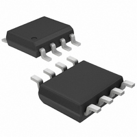
MAX5035BUSA+ Maxim Integrated Products, MAX5035BUSA+ Datasheet - Page 11

MAX5035BUSA+
Manufacturer Part Number
MAX5035BUSA+
Description
IC DC-DC CONV HI EFF 8-SOIC
Manufacturer
Maxim Integrated Products
Type
Step-Down (Buck)r
Datasheet
1.MAX5035AUSA.pdf
(17 pages)
Specifications of MAX5035BUSA+
Internal Switch(s)
Yes
Synchronous Rectifier
No
Number Of Outputs
1
Voltage - Output
5V
Current - Output
1A
Frequency - Switching
125kHz
Voltage - Input
7.5 ~ 76 V
Operating Temperature
0°C ~ 85°C
Mounting Type
Surface Mount
Package / Case
8-SOIC (3.9mm Width)
Power - Output
471mW
Lead Free Status / RoHS Status
Lead free / RoHS Compliant
The MAX5035 features internal compensation for opti-
mum closed-loop bandwidth and phase margin. With
the preset compensation, it is strongly advised to sense
the output immediately after the primary LC.
The choice of an inductor is guided by the voltage dif-
ference between V
current, and the operating frequency of the circuit. Use
an inductor with a minimum value given by:
where:
I
f
tor with a maximum saturation current rating equal to at
least the peak switch current limit (I
with low DC resistance for higher efficiency.
The MAX5035 requires an external Schottky rectifier as
a freewheeling diode. Connect this rectifier close to the
device using short leads and short PC board traces.
Choose a rectifier with a continuous current rating
greater than the highest expected output current. Use a
rectifier with a voltage rating greater than the maximum
expected input voltage, V
Schottky rectifier for proper operation and high efficien-
cy. Avoid higher than necessary reverse-voltage
Schottky rectifiers that have higher forward-voltage
drops. Use a Schottky rectifier with forward-voltage
Table 1. Diode Selection
SW
OUTMAX
7.5 to 36
7.5 to 56
7.5 to 76
V
IN
is the operating frequency of 125kHz. Use an induc-
(V)
is the maximum output current required, and
DIODE PART NUMBER
MBRS240, MBRS1540
MBRD360, MBR3060
50SQ100, 50SQ80
L
=
MBRM5100
15MQ040N
CMSH3-60
30BQ060
B240A
B360A
. 0 3
______________________________________________________________________________________
B240
IN
(
V
IN
D
×
and V
=
I
OUTMAX
−
IN
V
. Use a low forward-voltage
V
V
OUT
Selecting a Rectifier
IN
OUT
OUT
1A, 76V, High-Efficiency MAXPower
Inductor Selection
, the required output
)
Central Semiconductor
Central Semiconductor
×
×
LIM
MANUFACTURER
ON Semiconductor
ON Semiconductor
f
D
SW
Diodes, Inc.
Diodes, Inc.
Diodes, Inc.
). Use inductors
IR
IR
IR
Step-Down DC-DC Converter
drop (V
current to avoid forward biasing of the internal body
diode (LX to ground). Internal body diode conduction
may cause excessive junction temperature rise and
thermal shutdown. Use Table 1 to choose the proper
rectifier at different input voltages and output current.
The discontinuous input-current waveform of the buck
converter causes large ripple currents in the input
capacitor. The switching frequency, peak inductor cur-
rent, and the allowable peak-to-peak voltage ripple that
reflects back to the source dictate the capacitance
requirement. The MAX5035 high switching frequency
allows the use of smaller-value input capacitors.
The input ripple is comprised of ΔV
capacitor discharge) and ΔV
the capacitor). Use low-ESR aluminum electrolytic
capacitors with high ripple-current capability at the input.
Assuming that the contribution from the ESR and capaci-
tor discharge is equal to 90% and 10%, respectively, cal-
culate the input capacitance and the ESR required for a
specified ripple using the following equations:
I
and f
For example, at V
input capacitance are calculated for the input peak-to-
peak ripple of 100mV or less yielding an ESR and
capacitance value of 80mΩ and 51μF, respectively.
Low-ESR, ceramic, multilayer chip capacitors are recom-
mended for size-optimized application. For ceramic
capacitors, assume the contribution from ESR and capaci-
tor discharge is equal to 10% and 90%, respectively.
The input capacitor must handle the RMS ripple current
without significant rise in temperature. The maximum
capacitor RMS current occurs at about 50% duty cycle.
where
OUT
SW
is the maximum output current of the converter
:
FB
is the oscillator switching frequency (125kHz).
) less than 0.45V at +25°C and maximum load
ESR
C
ΔI
IN
L
IN
IN
=
=
= 48V, V
(
D
=
I
V
OUT
IN
=
⎛
⎝ ⎜
Δ
Input Bypass Capacitor
V
I
V
OUT
IN
−
V
Q
ESR
× D D
Δ
V
V
OUT
OUT
IN
V
OUT
×
×
ESR
+
f
(caused by the ESR of
f
SW
(
Δ
SW
1−
)
= 3.3V, the ESR and
2
I
L L
×
D
Q
×
⎞
⎠ ⎟
V
)
(caused by the
L
OUT
,
11


