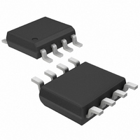
MAX757CSA+ Maxim Integrated Products, MAX757CSA+ Datasheet - Page 5

MAX757CSA+
Manufacturer Part Number
MAX757CSA+
Description
IC DC-DC CONV 8-SOIC
Manufacturer
Maxim Integrated Products
Type
Step-Up (Boost)r
Datasheet
1.MAX756CPA.pdf
(8 pages)
Specifications of MAX757CSA+
Internal Switch(s)
Yes
Synchronous Rectifier
No
Number Of Outputs
1
Voltage - Output
2.7 ~ 5.5 V
Current - Output
300mA
Frequency - Switching
500kHz
Voltage - Input
0.7 ~ 5.5 V
Operating Temperature
0°C ~ 70°C
Mounting Type
Surface Mount
Package / Case
8-SOIC (3.9mm Width)
Power - Output
471mW
Output Voltage
5.5 V
Output Current
0.3 mA
Input Voltage
5.5 V
Supply Current
0.06 A
Switching Frequency
500 KHz
Mounting Style
SMD/SMT
Maximum Operating Temperature
+ 70 C
Minimum Operating Temperature
0 C
Lead Free Status / RoHS Status
Lead free / RoHS Compliant
The MAX756/MAX757 combine a switch-mode regulator
with an N-channel MOSFET, precision voltage reference,
and power-fail detector in a single monolithic device.
The MOSFET is a “sense-FET” type for best efficiency,
and has a very low gate threshold voltage to ensure
start-up under low-battery voltage conditions (1.1V typ).
A unique minimum off time, current-limited, pulse-frequen-
cy modulation (PFM) control scheme is a key feature of
the MAX756/MAX757. This PFM scheme combines the
advantages of pulse-width modulation (PWM) (high output
power and efficiency) with those of a traditional PFM
pulse-skipper (ultra-low quiescent currents). There is no
oscillator; at heavy loads, switching is accomplished
through a constant peak-current limit in the switch, which
allows the inductor current to self-oscillate between this
peak limit and some lesser value. At light loads, switching
frequency is governed by a pair of one-shots, which set a
minimum off-time (1µs) and a maximum on-time (4µs).
The switching frequency depends on the load and the
input voltage, and can range as high as 500kHz.
The peak switch current of the internal MOSFET power
switch is fixed at 1A ±0.2A. The switch's on resistance
is typically 0.5Ω, resulting in a switch voltage drop
(V
value of V
Conventional PWM converters generate constant-fre-
quency switching noise, whereas this architecture pro-
duces variable-frequency switching noise. However,
the noise does not exceed the switch current limit times
the filter-capacitor equivalent series resistance (ESR),
unlike conventional pulse-skippers.
The precision voltage reference is suitable for driving
external loads such as an analog-to-digital converter.
It has guaranteed 250µA source-current and 20µA
sink-current capability. The reference is kept alive
even in shutdown mode. If the reference drives an
external load, bypass it with 0.22µF to GND. If the ref-
erence is unloaded, bypass it with at least 0.1µF.
The control inputs (3/5, SHDN) are high-impedance
MOS gates protected against ESD damage by normally
reverse-biased clamp diodes. If these inputs are dri-
ven from signal sources that exceed the main supply
_______________Detailed Description
SW
) of about 500mV under high output loads. The
SW
decreases with light current loads.
_______________________________________________________________________________________
Modulation Control Scheme
Control-Logic Inputs
Operating Principle
Voltage Reference
Pulse-Frequency
3.3V/5V/Adjustable-Output,
Step-Up DC-DC Converters
voltage, the diode current should be limited by a series
resistor (1MΩ suggested). The logic input threshold
level is the same (approximately 1V) in both 3.3V and
5V modes. Do not leave the control inputs floating.
The MAX756 output voltage can be selected to 3.3V or
5V under logic control, or it can be left in one mode or
the other by tying 3/5 to GND or OUT. Efficiency varies
depending upon the battery and the load, and is typi-
cally better than 80% over a 2mA to 200mA load range.
The device is internally bootstrapped, with power
derived from the output voltage (via OUT). When the
output is set at 5V instead of 3.3V, the higher internal
supply voltage results in lower switch-transistor on
resistance and slightly greater output power.
Bootstrapping allows the battery voltage to sag to less
than 1V once the system is started. Therefore, the bat-
tery voltage range is from V
(where V
If the battery voltage exceeds the programmed output
voltage, the output will follow the battery voltage. In
many systems this is acceptable; however, the output
voltage must not be forced above 7V.
The output voltage of the MAX757 is set by two resis-
tors, R1 and R2 (Figure 1), which form a voltage divider
between the output and the FB pin. The output voltage
is set by the equation:
where V
To simplify resistor selection:
Since the input bias current at FB has a maximum
value of 100nA, large values (10kΩ to 200kΩ) can be
used for R1 and R2 with no significant loss of accuracy.
For 1% error, the current through R1 should be at least
100 times FB’s bias current.
The MAX756/MAX757 contain on-chip circuitry for low-
battery detection. If the voltage at LBI falls below the reg-
ulator’s internal reference voltage (1.25V), LBO (an open-
drain output) sinks current to GND. The low-battery mon-
itor's threshold is set by two resistors, R3 and R4 (Figure
1), which forms a voltage divider between the input volt-
age and the LBI pin. The threshold voltage is set by R3
and R4 using the following equation:
__________________Design Procedure
REF
D
V
R1 = (R2) [(V
R3 = [(V
is the forward drop of the Schottky rectifier).
OUT
= 1.25V.
= (V
IN
REF
/ V
) [(R2 + R1) / R2]
Output Voltage Selection
REF
OUT
Low-Battery Detection
) - 1] (R4)
/ V
OUT
REF
) - 1]
+ V
D
to less than 1V
5


