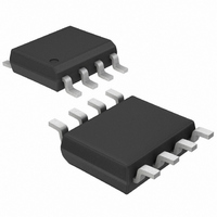
MAX889TESA+ Maxim Integrated Products, MAX889TESA+ Datasheet - Page 2

MAX889TESA+
Manufacturer Part Number
MAX889TESA+
Description
IC CHRG PUMP 200MA 8-SOIC
Manufacturer
Maxim Integrated Products
Type
Switched Capacitor (Charge Pump), Invertingr
Datasheet
1.MAX890LESAT.pdf
(8 pages)
Specifications of MAX889TESA+
Internal Switch(s)
Yes
Synchronous Rectifier
No
Number Of Outputs
1
Voltage - Output
-2.5 ~ -5.5 V
Current - Output
200mA
Frequency - Switching
2MHz
Voltage - Input
2.7 ~ 5.5 V
Operating Temperature
-40°C ~ 85°C
Mounting Type
Surface Mount
Package / Case
8-SOIC (3.9mm Width)
Power - Output
471mW
Function
Inverting
Output Voltage
- 2.5 V to - 5.5 V
Output Current
200 mA (Min)
Maximum Operating Temperature
+ 85 C
Minimum Operating Temperature
- 40 C
Mounting Style
SMD/SMT
Lead Free Status / RoHS Status
Lead free / RoHS Compliant
ABSOLUTE MAXIMUM RATINGS
IN to GND .................................................................-0.3V to +6V
FB, SHDN, CAP+ to GND ............................-0.3V to (V
AGND to GND .......................................................-0.3V to +0.3V
OUT to GND .............................................................-6V to +0.3V
CAP- to GND ............................................(V
Continuous Output Current ...............................................250mA
Output Short-Circuit Duration ........................................Indefinite
High-Frequency, Regulated,
200mA, Inverting Charge Pump
Stresses beyond those listed under “Absolute Maximum Ratings” may cause permanent damage to the device. These are stress ratings only, and functional
operation of the device at these or any other conditions beyond those indicated in the operational sections of the specifications is not implied. Exposure to
absolute maximum rating conditions for extended periods may affect device reliability.
ELECTRICAL CHARACTERISTICS
(V
2
Supply Voltage Range
Output Voltage Range
Maximum Output Current
Quiescent Supply
Current (Free-Run Mode)
Quiescent Supply
Current (Regulated Mode)
Shutdown Supply Current
Open-Loop Output
Resistance (Free-Run Mode)
Output Resistance
SHDN, FB Input Bias Current
FB Input Offset Voltage
Load Regulation
IN Undervoltage Lockout
Threshold
SHDN Logic High
SHDN Logic Low
Switching Frequency
Thermal Shutdown Threshold
IN
_______________________________________________________________________________________
= V
SHDN
PARAMETER
= +5V, capacitors from Table 1, T
I
Q(REGULATED)
I
Q(FREE-RUN)
I
OUT(MAX)2
R
I
SYMBOL
OUT(MAX)1
O(REG1)
I
V
f
SHDN
OSC
V
V
R
V
OUT
IN
IH
IL
O
OUT
- 0.3V) to +0.3V
A
= 0°C to +85°C, unless otherwise noted. Typical values are at T
R
R
V
V
No load, V
No load, V
-3.3V
V
V
V
I
I
V
V
MAX889R
MAX889S
MAX889T
Junction temperature rising
(15°C hysteresis)
LOAD
OUT
IN
IN
IN
FB
OUT
IN
IN
LOAD
SHDN
LOAD
+ 0.3V)
= 5V, V
= 3.3V, V
rising (30mV hysteresis)
= +2.7V to +5.5V
= V
= 0 to 200mA
regulated to -3.3V
= 0
= 100Ω
= 0
= 100Ω
IN
FB =
OUT
OUT
OUT
CONDITIONS
regulated to
V
= -3.3V
IN
Continuous Power Dissipation (T
Operating Temperature Range...........................-40°C to +85°C
Junction Temperature ......................................................+150°C
Storage Temperature Range .............................-65°C to +150°C
Lead Temperature (soldering, 10s) ................................+300°C
= -2.5V
8-Pin SO (derate 5.88mW/°C above +70°C)...............471mW
MAX889R
MAX889S
MAX889T
MAX889R
MAX889S
MAX889T
0.7 x V
0.375
0.75
MIN
-2.5
200
145
2.7
2.3
1.5
A
IN
= +70°C)
TYP
0.05
160
3.3
5.5
0.1
2.0
0.5
12
24
11
±3
10
6
1
2
A
0.3 x V
= +25°C.)
MAX
0.62
1.25
-V
±35
5.5
4.5
2.6
2.5
12
24
48
12
22
50
±1
7
IN
IN
UNITS
MHz
mA
mA
mA
mV
mV
µA
µA
°C
Ω
Ω
V
V
V
V


