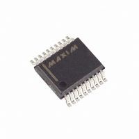
MAX1623EAP+ Maxim Integrated Products, MAX1623EAP+ Datasheet - Page 9

MAX1623EAP+
Manufacturer Part Number
MAX1623EAP+
Description
IC REG LV SYNC 3A STEPDWN 20SSOP
Manufacturer
Maxim Integrated Products
Type
Step-Down (Buck)r
Datasheet
1.MAX1623EAP.pdf
(12 pages)
Specifications of MAX1623EAP+
Internal Switch(s)
Yes
Synchronous Rectifier
Yes
Number Of Outputs
1
Voltage - Output
1.1 ~ 3.8 V
Current - Output
3A
Frequency - Switching
Up to 350kHz
Voltage - Input
4.5 ~ 5.5 V
Operating Temperature
-40°C ~ 85°C
Mounting Type
Surface Mount
Package / Case
20-SSOP
Power - Output
1.3W
Output Voltage
1.1 V to 3.8 V
Input Voltage
4.5 V to 5.5 V
Supply Current
400 uA
Switching Frequency
350 KHz
Maximum Operating Temperature
+ 85 C
Minimum Operating Temperature
- 40 C
Lead Free Status / RoHS Status
Lead free / RoHS Compliant
A high capacitor value maintains a constant average
output voltage but slows the loop response to changes
in output voltage. A low capacitor value speeds up the
loop response to changes in output voltage. Choose
the capacitor value that results in optimal performance.
The current-sense circuit enables when the PMOS
power switch is on. This circuit’s corresponding output
voltage feeds three separate comparators: the skip cur-
rent comparator (1.25A), the maximum current com-
parator (4.15A), and the PWM current comparator (see
the Modes of Operation section).
The MAX1623 features a programmable off-time that is
set by R
a 110kΩ resistor from TOFF to GND achieves a 1µs
(nominal) off-time. The off-time is inversely proportional
to R
t
Typical Operating Characteristics). To set the switching
frequency when the inductor operates in continuous-
conduction mode, the off-time has to be set to:
where:
t
V
V
Figure 3. Adjustable Output Voltage
OFF
Synchronous Rectification and Internal Switches
OFF
I
O
= input voltage
= output voltage
TOFF
= the programmed off-time
is adjustable between 0.5µs to 4µs (see the
TOFF
according to the formula:
t
MAX1623
OFF
3A, Low-Voltage, Step-Down Regulator with
connected from TOFF to GND. Connecting
t
=
OFF
PGND
GND
_______________________________________________________________________________________
f V
LX
FB
(
= R
V
Programming the Off-Time
I
I
R1 = 10kΩ to 500kΩ
R2 = R1(V
V
Oscillator Frequency and
−
REF
−
TOFF
V
V
PCH
= 1.1V
O
OUT
/ 110k (µs)
−
+
/ V
V
REF
PCH
V
Current Limiting
NCH
- 1)
)
R2
R1
V
OUT
f = desired switching frequency during continuous
V
V
Switching frequency decreases as load current is
decreased below the 625mA Idle Mode trip point.
The 1.10V internal reference (available at REF) is accu-
rate to ±1.5% over the -40°C to +85°C operating range,
making it useful as a precision system reference. Bypass
the reference to ground with a minimum 0.1µF ceramic
capacitor. For low noise and jitter performance, use a
0.47µF ceramic capacitor. The reference can supply up
to 10µA for external loads. However, if tight accuracy
specifications for either reference or the main output are
essential, avoid reference loads in excess of 5µA.
Loading the reference reduces the main output voltage
slightly, according to the reference-voltage load-regula-
tion error.
To prevent the MAX1623 from false output regulation,
the internal PMOS and NMOS switches will not switch
on until all of the following conditions are true: the sup-
ply voltage is above the undervoltage lockout thresh-
old, SHDN is pulled high, the internal reference voltage
is at 75% of its nominal (1.1V) value, and the die tem-
perature is below +145°C. When the above conditions
are satisfied, the MAX1623 will regulate the output volt-
age to the selected level. The MAX1623 typically starts
up in 1ms for full output load.
Thermal overload protection limits the MAX1623’s total
power dissipation. When the junction temperature
reaches T
cool down. Switching resumes after the IC’s junction
temperature decreases by 20°C. If the thermal overload
condition persists, the output pulses on and off.
Thermal overload protection is designed to protect the
MAX1623 during fault conditions, such as an output
short circuit.
Junction to ambient thermal resistance (θ
depends on the amount of copper area immediately
surrounding the IC’s leads. The MAX1623 evaluation kit
has 0.8in
sured to have 45°C/W of thermal resistance with no air
PCH
NCH
inductor current
= the voltage drop across the internal P-channel
= the voltage drop across the internal N-channel
switch
synchronous rectifier
2
j
= +145°C, the device turns off, allowing it to
of copper area. θ
Thermal Shutdown and
JA
Overload Conditions
Thermal Resistance
Internal Reference
on this board was mea-
JA
Start-Up
) strongly
9


