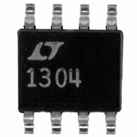
LT1304CS8-5 Linear Technology, LT1304CS8-5 Datasheet - Page 8

LT1304CS8-5
Manufacturer Part Number
LT1304CS8-5
Description
IC DC/DC CONV STEP-UP 5V 8-SOIC
Manufacturer
Linear Technology
Type
Step-Up (Boost)r
Datasheet
1.LT1304CS8-5PBF.pdf
(16 pages)
Specifications of LT1304CS8-5
Internal Switch(s)
Yes
Synchronous Rectifier
No
Number Of Outputs
1
Voltage - Output
5V
Current - Output
200mA
Frequency - Switching
300kHz
Voltage - Input
1.5 ~ 8 V
Operating Temperature
0°C ~ 70°C
Mounting Type
Surface Mount
Package / Case
8-SOIC (3.9mm Width)
Power - Output
500mW
Lead Free Status / RoHS Status
Contains lead / RoHS non-compliant
Available stocks
Company
Part Number
Manufacturer
Quantity
Price
Company:
Part Number:
LT1304CS8-5
Manufacturer:
LT
Quantity:
10 000
OPERATIO
LT1304/LT1304-3.3/LT1304-5
If the full power capability of the LT1304 is not required,
peak switch current can be limited by connecting a resistor
R
switch current is reduced to approximately 500mA. Smaller
power components can then be used. The graph in Figure
6 shows switch current vs R
Layout/Input Bypassing
The LT1304’s high speed switching mandates careful
attention to PC board layout. Suggested component place-
ment is shown in Figure 7. The input supply must have low
impedance at AC and the input capacitor should be placed
as indicated in the figure. The value of this capacitor
depends on how close the input supply is to the IC. In
situations where the input supply is more than a few
inches away from the IC, a 47 F to 100 F solid tantalum
8
LIM
Figure 5. Start-Up Response with 1 F/1M Components
in Figure 2 Added. Input Current Is More Controlled. V
Reaches 5V in 6ms. Output Drives 20mA Load
from the I
500mA/DIV
10V/DIV
2V/DIV
Figure 6. Peak Switch Current vs R
V
V
SHDN
OUT
1000
I
900
800
700
600
500
400
IN
10
LIM
U
pin to ground. With R
R
1ms/DIV
LIM
LIM
100
(k )
resistor value.
LIM
LIM
1304 F06
1304 F05
Value
1000
= 22k, peak
OUT
bypass capacitor is required. If the input supply is close to
the IC, a 1 F ceramic capacitor can be used instead. The
LT1304 switches current in 1A pulses, so a low impedance
supply must be available. If the power source (for example,
a 2 AA cell battery) is within 1 or 2 inches of the IC, the
battery itself provides bulk capacitance and the 1 F ce-
ramic capacitor acts to smooth voltage spikes at switch
turn-on and turn-off. If the power source is far away from
the IC, inductance in the power source leads results in high
impedance at high frequency. A local high capacitance
bypass is then required to restore low impedance at the IC.
Low-Battery Detector
The LT1304 contains an independent low-battery detector
that remains active when the device is shut down. This
detector, actually a hysteretic comparator, has an open
collector output that can sink up to 500 A. The compara-
tor also operates below the switcher’s undervoltage lock-
out threshold, operating until V
1.4V. Figure 8 illustrates the input/output characteristic of
the detector. Hysteresis is clearly evident in the figure.
V
IN
Figure 7. Suggested Layout for Best Performance. Input
Capacitor Placement as Shown Is Highly Recommended.
Switch Trace (Pin 4) Copper Area Is Minimized
V
OUT
+
GND (BATTERY AND LOAD RETURN)
C
OUT
1
2
3
4
SHUTDOWN
LT1304
+
IN
C
IN
reaches approximately
8
7
6
5
1304 F07


