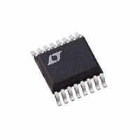
LTC1550CGN Linear Technology, LTC1550CGN Datasheet

LTC1550CGN
Specifications of LTC1550CGN
Available stocks
Related parts for LTC1550CGN
LTC1550CGN Summary of contents
Page 1
... High Output Current 10mA, V Output Regulation: 5% Available in SO-8 and 16-Lead SSOP U APPLICATIONS GaAs FET Bias Generators Negative Supply Generators Battery-Powered Systems Single Supply Applications , LTC and LT are registered trademarks of Linear Technology Corporation. U TYPICAL APPLICATION – 4.1V Generator with 1mV SHDN SENSE ...
Page 2
... V 6.5V 20mA CC OUT 2.7V V 6.5V 5mA CC OUT 3.1V V 6.5V 10mA CC OUT 3.75V V 6.5V 20mA CC OUT ORDER PART NUMBER SHDN 14 LTC1550CGN REG 13 SENSE LTC1550IGN 12 ADJ 11 CP OUT PART MARKING 9 NC 1550 = 150 MIN TYP MAX 2.7 6.5 4.5 6.5 1.24 4.25 7 (LTC1551) 0 ...
Page 3
... Output Regulation OUT (LTC1550CGN/LTC1550IGN) V Output Regulation OUT (LTC1550CGN/LTC1550IGN) V Output Regulation OUT (LTC1550CGN/LTC1550IGN) V Output Regulation OUT (LTC1550CGN/LTC1550IGN) V Output Regulation OUT (LTC1550CS8-4.1/LTC1551CS8-4.1) I Output Short-Circuit Current SC V Output Ripple Voltage RIPPLE The denotes specifications which apply over the specified temperature range. Note 1: Absolute Maximum Ratings are those values beyond which the life of a device may be impaired. Note 2: All currents into device pins are positive ...
Page 4
LTC1550/LTC1551 W U TYPICAL PERFORMANCE CHARACTERISTICS Maximum Output Current vs Supply Voltage 4.50 4.75 5.00 5.25 5.50 5.75 6.00 6.25 6.50 SUPPLY VOLTAGE (V) ...
Page 5
... CC CC 4.5V and 6.5V for the fixed voltage LTC1550CS8-4.1/ LTC1551CS8-4.1. The adjustable voltage LTC1550CGN/ LTC1550IGN operates with a VCC range of 2.7V to 6.5V. Output voltage and output load current conditions depend on the VCC supply voltage. Consult the Electrical Charac- teristics table and Typical Performance Characteristics for guaranteed test points ...
Page 6
... The LTC1550CS8/LTC1551CS8 provide a regulated, low ripple – 4.1V output 10mA load current from a single 5V supply. The LTC1550CGN provides a regulated, low ripple adjustable output. Output load current for the adjustable version depends on the input/output voltage combination. ...
Page 7
... W U Adjustable Hook- OUT The LTC1550CGN is available in an adjustable output version in a 16-pin SSOP package. The output voltage is set with a resistor divider from GND to SENSE/V (Figure 1). Note that the internal reference and the internal feedback amplifier are set positive-output regula- tor referenced to the SENSE pin, not a negative regulator referenced to ground ...
Page 8
LTC1550/LTC1551 U U APPLICATIONS INFORMATION output capacitors provide lower output ripple. To keep ripple below 1mV , greater, with a 0.1 F ceramic P-P capacitor in parallel, is required. At least 4 required at the ...
Page 9
U U APPLICATIONS INFORMATION noise – 4.1V generator which uses a ferrite bead output filter to achieve better than 1mV ripple. The corresponding spectrum and spot noise plots for this circuit are shown in the Typical Performance Characteristics section. Output ...
Page 10
LTC1550/LTC1551 PACKAGE DESCRIPTION 0.0075 – 0.0098 (0.191 – 0.249) 0.016 – 0.050 (0.406 – 1.270) * DIMENSION DOES NOT INCLUDE MOLD FLASH. MOLD FLASH SHALL NOT EXCEED 0.006" (0.152mm) PER SIDE ** DIMENSION DOES NOT INCLUDE INTERLEAD FLASH. INTERLEAD FLASH ...
Page 11
... FLASH SHALL NOT EXCEED 0.010" (0.254mm) PER SIDE Information furnished by Linear Technology Corporation is believed to be accurate and reliable. However, no responsibility is assumed for its use. Linear Technology Corporation makes no represen- tation that the interconnection of its circuits as described herein will not infringe on existing patent rights. ...
Page 12
... CP OUT C CP LTC1550 0 GND 5 – C1 FERRITE BEAD C OUT 0.1 F COMMENTS 100mA Switched-Capacitor Converter Selectable Fixed Output Voltages Synchronizable Up to 2MHz System Clock – 4. GaAs 0.1 F TRANSMITTER 1550/51 TA03 15501fa LT/TP 0897 REV A 4K • PRINTED IN USA LINEAR TECHNOLOGY CORPORATION 1996 ...


