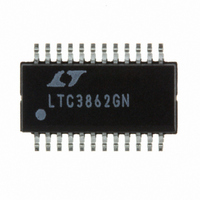
LTC3862IGN#PBF Linear Technology, LTC3862IGN#PBF Datasheet - Page 27

LTC3862IGN#PBF
Manufacturer Part Number
LTC3862IGN#PBF
Description
IC CTRLR DC/DC STPUP 24SSOP
Manufacturer
Linear Technology
Type
Step-Up (Boost)r
Datasheet
1.LTC3862EGNPBF.pdf
(40 pages)
Specifications of LTC3862IGN#PBF
Internal Switch(s)
No
Synchronous Rectifier
No
Number Of Outputs
1
Voltage - Output
1.22 ~ 200 V
Current - Output
50mA
Frequency - Switching
300kHz
Voltage - Input
4 ~ 36 V
Operating Temperature
-40°C ~ 125°C
Mounting Type
Surface Mount
Package / Case
24-SSOP
Primary Input Voltage
36V
No. Of Outputs
1
Output Current
50mA
No. Of Pins
24
Operating Temperature Range
-40°C To +125°C
Msl
MSL 1 - Unlimited
Supply Voltage Range
4V To 36V
Rohs Compliant
Yes
Lead Free Status / RoHS Status
Lead free / RoHS Compliant
Power - Output
-
APPLICATIONS INFORMATION
result, some iterative calculation is normally required to
determine a reasonably accurate value.
The power dissipated by the MOSFET in a multi-phase
boost converter with n phases is:
The fi rst term in the equation above represents the I
losses in the device, and the second term, the switching
losses. The constant, k = 1.7, is an empirical factor inversely
related to the gate drive current and has the dimension
of 1/current.
The ρ
the R
Figure 19 illustrates the variation of normalized R
over temperature for a typical power MOSFET.
From a known power dissipated in the power MOSFET, its
junction temperature can be obtained using the following
formula:
Figure 19. Normalized Power MOSFET R
T
P
J
FET
DS(ON)
= T
T
term accounts for the temperature coeffi cient of
=
A
⎛
⎜
⎝
+ P
+
2.0
1.5
1.0
0.5
n
0
of the MOSFET, which is typically 0.4%/ºC.
–50
k V
• –
FET
(
I
•
O MAX
1
(
• R
OUT
D
JUNCTION TEMPERATURE (°C)
TH(JA)
MAX
0
2
)
•
n
)
⎞
⎟
⎠
• –
2
(
I
50
O MAX
1
•
(
R
DS ON
D
MAX
(
)
100
DS(ON)
)
)
•
•
D
3862 F19
C
MAX
RSS
150
vs Temperature
•
•
ρ ρ
f
T
DS(ON)
2
R
The R
the R
the case to the ambient temperature (R
of T
used in the iterative calculation process.
It is tempting to choose a power MOSFET with a very low
R
so, however, the gate charge Q
higher, which increases switching and gate drive losses.
Since the switching losses increase with the square of
the output voltage, applications with a low output voltage
generally have higher MOSFET conduction losses, and
high output voltage applications generally have higher
MOSFET switching losses. At high output voltages, the
highest effi ciency is usually obtained by using a MOSFET
with a higher R
can easily be split into two components (conduction and
switching) and entered into a spreadsheet, in order to
compare the performance of different MOSFETs.
Programming the Current Limit
The peak sense voltage threshold for the LTC3862 is 75mV
at low duty cycle and with a normalized slope gain of
1.00, and is measured from SENSE
illustrates the change in the sense threshold with varying
duty cycle and slope gain.
DS(ON)
J
TH(JC)
can then be compared to the original, assumed value
TH(JA)
in order to reduce conduction losses. In doing
Figure 20. Maximum Sense Voltage Variation
with Duty Cycle and Slope Gain
80
75
70
65
60
55
50
for the device plus the thermal resistance from
to be used in this equation normally includes
0
DS(ON)
10
20
30
and lower Q
DUTY CYCLE (%)
40
SLOPE = 1
SLOPE = 1.66
50
60
G
SLOPE = 0.625
70
is usually signifi cantly
G
+
. The equation above
to SENSE
80
TH(CA)
LTC3862
90
3862 F20
100
). This value
–
. Figure 20
27
3862fb


