LM3524DM/NOPB National Semiconductor, LM3524DM/NOPB Datasheet - Page 5
LM3524DM/NOPB
Manufacturer Part Number
LM3524DM/NOPB
Description
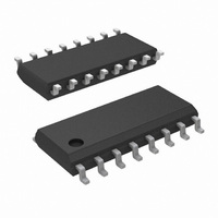
IC REGULATOR PWM SWITCHER 16SOIC
Manufacturer
National Semiconductor
Type
Step-Down (Buck), Step-Up (Boost), Flybackr
Datasheet
1.LM2524DNNOPB.pdf
(22 pages)
Specifications of LM3524DM/NOPB
Internal Switch(s)
Yes
Synchronous Rectifier
No
Number Of Outputs
1
Voltage - Output
5V
Current - Output
200mA
Frequency - Switching
550kHz
Voltage - Input
8 ~ 40 V
Operating Temperature
0°C ~ 125°C
Mounting Type
Surface Mount
Package / Case
16-SOIC (3.9mm Width)
Power - Output
1W
Lead Free Status / RoHS Status
Lead free / RoHS Compliant
Other names
*LM3524DM
*LM3524DM/NOPB
LM3524DM
*LM3524DM/NOPB
LM3524DM


SHUT
V
I
OUTPUT
V
I
V
V
t
t
SUPPLY
V
T
I
SD
CES
R
F
IN
SD
CES
CESAT
EO
IN
Symbol
Note 1: Unless otherwise stated, these specifications apply for T
85°C and LM3524D is 0°C to 70°C. V
Note 2: For operation at elevated temperatures, devices in the N package must be derated based on a thermal resistance of 86°C/W, junction to ambient. Devices
in the M package must be derated at 125°C/W, junction to ambient.
Note 3: Tested limits are guaranteed and 100% tested in production.
Note 4: Design limits are guaranteed (but not 100% production tested) over the indicated temperature and supply voltage range. These limits are not used to
calculate outgoing quality level.
Note 5: Absolute maximum ratings indicate limits beyond which damage to the device may occur. DC and AC electrical specifications do not apply when operating
the device beyond its rated operating conditions.
Note 6: Pins 1, 4, 7, 8, 11, and 14 are grounded; Pin 2 = 2V. All other inputs and outputs open.
Note 7: The value of a C
in this test. NPO ceramic or polypropylene can also be used.
Note 8: OSC amplitude is measured open circuit. Available current is limited to 1 mA so care must be exercised to limit capacitive loading of fast pulses.
DOWN
CHARACTERISTICS
SECTION
Common Mode
Voltage Range
High Input
Voltage
High Input
Current
Collector Emitter
Voltage Breakdown
Collector Leakage
Current
Saturation
Voltage
Emitter Output
Voltage
Rise Time
Fall Time
Input Voltage
Range
Thermal Shutdown (Note 2)
Temp.
Stand By Current
SECTION
Parameter
t
(EACH
capacitor can vary with frequency. Careful selection of this capacitor must be made for high frequency operation. Polystyrene was used
OUTPUT)
IN
SECTION
= 20V and f
V
V
150 mV
I
I
V
V
V
I
I
I
V
I
R
R
After Turn-on
V
(pin 10)
C
E
E
E
E
5
(Pin 2)
CE
CE
CE
IN
IN
C
C
≤
= 20 mA
= 200 mA
= 50 mA
= −250 μA
− V
= 2k
= 2k
= 20V,
= 40V (Note 6)
= 60V
= 55V
= 40V
100 μA
4
− V
= 300 mV
Conditions
OSC
(Pin 1)
= 20 kHz.
≥
A
= T
J
= 25°C. Boldface numbers apply over the rated temperature range: LM2524D is −40° to
−0.7
5
Typ
200
100
160
0.1
0.2
1.5
18
1
1
1
5
(Note 3)
Tested
Limit
LM2524D
0.5
1.5
0.5
2.2
55
50
17
40
10
8
(Note 4)
Design
Limit
−0.7
Typ
200
100
160
0.1
0.2
1.5
18
1
1
1
5
(Note 3)
Tested
LM3524D
Limit
0.5
1.5
0.7
2.5
40
50
17
40
10
8
(Note 4)
Design
Limit
www.national.com
μA
Units
V
V
V
V
V
V
V
V
V
mA
mA
ns
ns
°C
Max
Max
Max
Max
Min
Min
Min
Min
Min
Max
Related parts for LM3524DM/NOPB
Image
Part Number
Description
Manufacturer
Datasheet
Request
R

Part Number:
Description:
IC, REGULATING PWM, 16-SOIC
Manufacturer:
National Semiconductor
Datasheet:
Part Number:
Description:
National Semiconductor [8-Bit D/A Converter]
Manufacturer:
National Semiconductor
Datasheet:
Part Number:
Description:
National Semiconductor [Media Coprocessor]
Manufacturer:
National Semiconductor
Datasheet:
Part Number:
Description:
Digitally Controlled Tone and Volume Circuit with Stereo Audio Power Amplifier, Microphone Preamp Stage and National 3D Sound
Manufacturer:
National Semiconductor
Datasheet:
Part Number:
Description:
Digitally Controlled Tone and Volume Circuit with Stereo Audio Power Amplifier, Microphone Preamp Stage and National 3D Sound
Manufacturer:
National Semiconductor
Datasheet:
Part Number:
Description:
AC97 Rev 2 Codec with Sample Rate Conversion and National 3D Sound
Manufacturer:
National Semiconductor
Part Number:
Description:
Manufacturer:
National Semiconductor
Datasheet:
Part Number:
Description:
Manufacturer:
National Semiconductor
Datasheet:
Part Number:
Description:
General Purpose, Low Voltage, Low Power, Rail-to-Rail Output Operational Amplifiers
Manufacturer:
National Semiconductor
Datasheet:
Part Number:
Description:
8-bit 20 MSPS flash A/D converter.
Manufacturer:
National Semiconductor
Datasheet:
Part Number:
Description:
Low Noise Quad Operational Amplifier
Manufacturer:
National Semiconductor
Datasheet:
Part Number:
Description:
Quad Differential Line Receivers
Manufacturer:
National Semiconductor
Datasheet:
Part Number:
Description:
Quad High Speed Trapezoidal? Bus Transceiver
Manufacturer:
National Semiconductor
Datasheet:
Part Number:
Description:
Dual Line Receiver
Manufacturer:
National Semiconductor
Datasheet: