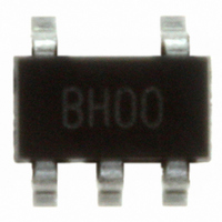
SC4503TSKTRT Semtech, SC4503TSKTRT Datasheet - Page 14

SC4503TSKTRT
Manufacturer Part Number
SC4503TSKTRT
Description
IC SW REG STEP-UP 1.4A TSOT23-5
Manufacturer
Semtech
Type
Step-Up (Boost), Sepicr
Datasheet
1.SC4503TSKTRT.pdf
(22 pages)
Specifications of SC4503TSKTRT
Internal Switch(s)
Yes
Synchronous Rectifier
No
Number Of Outputs
1
Voltage - Output
Adj to 27V
Current - Output
1.4A
Frequency - Switching
1.3MHz
Voltage - Input
2.5 ~ 20 V
Operating Temperature
-40°C ~ 85°C
Mounting Type
Surface Mount
Package / Case
TSOT-23-5, TSOT-5, TSOP-5
Lead Free Status / RoHS Status
Lead free / RoHS Compliant
Power - Output
-
Other names
SC4503TSKTR
Available stocks
Company
Part Number
Manufacturer
Quantity
Price
Company:
Part Number:
SC4503TSKTRT
Manufacturer:
TI
Quantity:
6 000
Part Number:
SC4503TSKTRT
Manufacturer:
SEMTECH/美国升特
Quantity:
20 000
Figures 7(a)-7(c) show the effects of different values of
inductance and feed-forward capacitance on transient re-
sponses. In a battery-operated system if C
the minimum V
will be stable over the entire input voltage range.
2007 Semtech Corp.
Figure 7.
POWER MANAGEMENT
Applications Information (Cont.)
0.5V/div
0.5A/div
0.5V/div
0.5A/div
0.5V/div
0.5A/div
Different inductances and feed-forward capaci-
tances affect the load transient responses of the
3.3V to 12V step-up converter in Figure 10(a).
I
OUT
is switched between 90mA and 280mA.
V
V
V
IN
OUT
OUT
OUT
I
I
I
L1
L1
L1
and the maximum load step, the converter
(b) L
(c) L
(a) L
1
1
1
= 5.6µH and C
= 3.3µH and C
= 5.6µH and C
40µs/div
40µs/div
40µs/div
4
4
4
= 3.3pF
4
= 2.7pF
= 2.2pF
is optimized for
14
Board Layout Considerations
In a step-up switching regulator, the output fi lter capacitor,
the main power switch and the rectifying diode carry pulse
currents with high di/dt. For jitter-free operation, the size of
the loop formed by these components should be minimized.
Since the power switch is integrated inside the SC4503,
grounding the output fi lter capacitor next to the SC4503
ground pin minimizes size of the high di/dt current loop.
The input bypass capacitors should also be placed close to
the input pins. Shortening the trace at the SW node reduces
the parasitic trace inductance. This not only reduces EMI
but also decreases switching voltage spikes.
Figure 8 shows how various external components are
placed around the SC4503.
The large surrounding ground plane acts as a heat sink
for the device.
Figure 8. Suggested PCB Layout for the SC4503.
VOUT
GND
R1
R2
C4
C2
FB
D1
SW
U1
C3
L1
SHDN/SS
C1
www.semtech.com
SC4503
R3
VIN
JP


