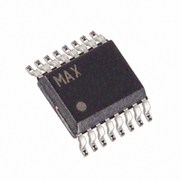
MAX1972EEE+ Maxim Integrated Products, MAX1972EEE+ Datasheet - Page 19

MAX1972EEE+
Manufacturer Part Number
MAX1972EEE+
Description
IC REG STP DWN 750MA 16-QSOP
Manufacturer
Maxim Integrated Products
Type
Step-Down (Buck)r
Datasheet
1.MAX1972EEE.pdf
(21 pages)
Specifications of MAX1972EEE+
Internal Switch(s)
Yes
Synchronous Rectifier
Yes
Number Of Outputs
2
Voltage - Output
1.5V, 1.8V, 2.5V, 3.3V, Adj
Current - Output
750mA
Frequency - Switching
1.4MHz
Voltage - Input
2.6 ~ 5.5 V
Operating Temperature
-40°C ~ 85°C
Mounting Type
Surface Mount
Package / Case
16-QSOP
Power - Output
667mW
Lead Free Status / RoHS Status
Lead free / RoHS Compliant
As the load current decreases, the modulator pole also
decreases; however, the modulator gain increases
accordingly, and the closed-loop unity-gain frequency
remains the same. Below is a numerical example to cal-
culate R
cuit of Figure 4, where:
Pick a closed-loop unity-gain frequency (f
The power modulator gain at fc is:
then:
G
x 3.80k/50k = 0.635
V
I
C
R
gm
gm
f
R
fp
10 x 10
fz
0.01] = 1.59MHz.
R
1.2 x 0.635) ≈ 62kΩ
C
x 10
OUT(MAX)
SWITCH
OUT
ESR
LOAD
MOD
C
OUT
ESR
C
Dual, 180° Out-of-Phase, 1.4MHz, 750mA Step-
MOD
EA
C
= V
= V
-6
= 2S
= 0.010Ω
/62k x 0.6 ≈ 680pF
= 2.5V
= 1/[2π C
= 10µF
(fc) = gmc x R
C
= 50µS
O
-6
= V
= 1/[2π C
OUT
/(gm
and C
= 1.4MHz
(4.167 + 0.01)] = 3.80kHz.
= 0.6A
OUT
EA
x (C
/I
C
OUT
OUT(MAX)
V
______________________________________________________________________________________
values of the typical application cir-
FB
OUT
OUT
Down Regulator with POR and RSI/PFO
R
G
ESR
/R
LOAD
MOD
(R
C
] = 1/[2π x 10 x 10
) x I
= 2.5V/0.6A = 4.167Ω
LOAD
(fc)) = 2.5/(50 x 10
x fp
OUT
+ R
MOD
(MAX) = 2.5 x 4.7
ESR
/f
c
)] = 1/[2π x
c
= 2 x 4.167
) of 50kHz.
-6
x
-6
x
Careful PCB layout is critical to achieve clean and sta-
ble operation. The switching power stage requires par-
ticular attention. Follow these guidelines for good PCB
layout:
1) Place decoupling capacitors as close to IC pins as
2) Input and output capacitors are connected to the
3) Keep the high-current paths as short and wide as
4) If possible, connect IN, LX1, LX2, and PGND sepa-
5) Ensure all feedback connections are short and
6) Route high-speed switching nodes away from sen-
possible. Keep power ground plane (connected to
PGND) and signal ground plane (connected to
GND) separate. Connect the two ground planes
together with a single connection from PGND to
GND.
power ground plane; all other capacitors are con-
nected to signal ground plane.
possible.
rately to a large land area to help cool the IC to fur-
ther improve efficiency and long-term reliability.
direct. Place the feedback resistors as close to the
IC as possible.
sitive analog areas (FB1, FB2, COMP1, COMP2).
Applications Information
PCB Layout
19


