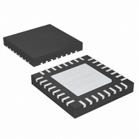
MAX5072ETJ+ Maxim Integrated Products, MAX5072ETJ+ Datasheet - Page 20

MAX5072ETJ+
Manufacturer Part Number
MAX5072ETJ+
Description
IC CONV BUCK/BOOST 32-TQFN
Manufacturer
Maxim Integrated Products
Type
Step-Down (Buck), Step-Up (Boost)r
Datasheet
1.MAX5072ETJ.pdf
(27 pages)
Specifications of MAX5072ETJ+
Internal Switch(s)
Yes
Synchronous Rectifier
No
Number Of Outputs
2
Voltage - Output
0.8 ~ 28 V
Current - Output
1A, 2A
Frequency - Switching
200kHz ~ 2.2MHz
Voltage - Input
4.5 ~ 23 V
Operating Temperature
-40°C ~ 85°C
Mounting Type
Surface Mount
Package / Case
32-TQFN Exposed Pad
Power - Output
2.76W
Output Voltage
5.2 V
Output Current
2 A
Input Voltage
5.5 V to 23 V
Supply Current
2.2 mA
Switching Frequency
1250 KHz
Mounting Style
SMD/SMT
Maximum Operating Temperature
+ 85 C
Minimum Operating Temperature
- 40 C
Lead Free Status / RoHS Status
Lead free / RoHS Compliant
2.2MHz, Dual-Output Buck or Boost
Converter with POR and Power-Fail Output
where
where V
MOSFET plus the voltage drop across the inductor
ESR. ∆I
calculated above. ∆V
to the capacitor discharge and ∆V
tion due to ESR of the capacitor.
For the boost converter, the output capacitor supplies
the load current when the main switch is ON. The
required output capacitance is high, especially at high-
er duty cycles. Also, the output capacitor ESR needs to
be low enough to minimize the voltage drop due to the
ESR while supporting the load current. Use the follow-
ing equation to calculate the output capacitor for a
specified output ripple tolerance.
I
due to the capacitor discharge and ∆V
bution due to the ESR of the capacitor. D
maximum duty cycle at minimum input voltage.
The MAX5072 includes a high-frequency, low R
switching MOSFET. At +85°C, the R
nal switch for converter 1 and converter 2 are 290mΩ
and 630mΩ, respectively. The DC loss is a function of
the RMS current in the switch while the switching loss is
a function of switching frequency and input voltage. Use
the following equations to calculate the RMS current,
DC loss, and switching loss of each converter. The
MAX5072 device is available in a thermally enhanced
package and can dissipate up to 2.7W at +70°C ambi-
20
O
is the load current, ∆V
______________________________________________________________________________________
L
DS
is the peak-to-peak inductor ripple current as
is the total voltage drop across the internal
C
∆I
IN
C
L
OUT
=
ESR
=
Q
ESR
(
4
V
is the portion of input ripple due
IN
=
×
=
Q
L
∆
Output Capacitor Selection
=
I
∆
−
O
∆
I
f
V
L
SW
×
V
is the portion of the ripple
∆
V
∆
Q
DS
ESR
V
×
I
I
×
L
f
ESR
O
SW
×
D
)
×
D
MAX
×
f
ESR
SW
∆
Power Dissipation
DS_ON
V
D
Q
ESR
is the contribu-
is the contri-
of the inter-
MAX
DS_ON
is the
ent temperature. The total power dissipation in the pack-
age must be limited so the junction temperature does not
exceed its absolute maximum rating of +150°C at maxi-
mum ambient temperature.
For the buck converter:
where
See the Electrical Characteristics table for the R
value.
Figure 7. Type II Compensation Network.
Figure 8. Type III Compensation Network
I
RMS
C
R
I
I
=
R
R
P
1
2
DC
(
V
I
OUT
R1
R2
2
DC
V
=
OUT
V
I
DC
REF
I
+I
2
I
PK
RMS
2
=
PK
V
-
+
REF
I
=
g
O
M
×
I
+(I
O
−
C
R
R
R
F
F
F
-
+
DS(ON)MAX
∆
+
C
DC
g
2
CF
M
I
L
∆
2
I
×
L
C
I
PK
F
COMP
))
C
CF
×
COMP
D
MAX
3
DS(ON)MAX


