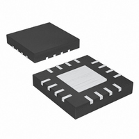
MAX5089ATE+ Maxim Integrated Products, MAX5089ATE+ Datasheet - Page 13

MAX5089ATE+
Manufacturer Part Number
MAX5089ATE+
Description
IC DC-DC CONV BUCK 16TQFN
Manufacturer
Maxim Integrated Products
Type
Step-Down (Buck)r
Datasheet
1.MAX5089ATE.pdf
(24 pages)
Specifications of MAX5089ATE+
Internal Switch(s)
Yes
Synchronous Rectifier
Yes
Number Of Outputs
1
Voltage - Output
0.6 ~ 20 V
Current - Output
2A
Frequency - Switching
200kHz ~ 2.2MHz
Voltage - Input
4.5 ~ 23 V
Operating Temperature
-40°C ~ 125°C
Mounting Type
Surface Mount
Package / Case
16-TQFN Exposed Pad
Power - Output
2.67W
Lead Free Status / RoHS Status
Lead free / RoHS Compliant
At high input-to-output differential, and high switching
frequency, the on-time drops to the order of 100ns.
Even though the MAX5088/MAX5089 can control the
on-time as low as 100ns, the internal current-limit circuit
may not detect the overcurrent within this time. In that
case, the output current during the fault may exceed the
current limit specified in the Electrical Characteristics
table. The MAX5088/MAX5089 may still be protected
against the output short-circuit fault through the
overtemperature shutdown. However, the output cur-
rent may be as high as 5.5A. If the minimum on-time for
a given frequency and duty cycle is less than 200ns,
choose the inductor with a saturation current of greater
than 5.5A.
RESET is an active-low open-drain output that pulls low
when V
RESET goes high impedance when V
92.5% of its nominal set point, the soft-start period is
complete, and the 200ms (typ) timeout period has
elapsed. Connect a pullup resistor from RESET to a
logic voltage or to V
at RESET can sink 3mA while providing a TTL-compati-
ble logic-low signal. Connect RESET to SGND or leave
unconnected when not used.
PGOOD is an open-drain, active-high output that pulls
low when V
and goes high impedance when V
92.5% its nominal set point. Connect a pullup resistor
from PGOOD to a logic voltage or to V
up to 3mA while still providing a TTL-compatible logic-low
output. Pulling EN low forces PGOOD low. Connect
PGOOD to SGND or leave unconnected when not used.
During a continuous output short-circuit or overload
condition, the power dissipation in the MAX5088/
MAX5089 can exceed its limit. The MAX5088/MAX5089
provide an internal thermal shutdown to turn off the
device when the die temperature reaches +170°C. A
thermal sensor monitors the die temperature and turns
OUT
OUT
falls below 92.5% of its nominal set point.
is below 92.5% of its nominal set point
Thermal-Overload Protection
______________________________________________________________________________________
L
. The internal open-drain MOSFET
Power-on Reset (
2.2MHz, 2A Buck Converters with an
Power-Good (PGOOD)
(MAX5088 Only)
(MAX5089 Only)
L
OUT
. PGOOD can sink
OUT
goes above
rises above
RESET )
Integrated High-Side Switch
the device on again when the die temperature reduces
by +25°C. During thermal shutdown, the internal power
MOSFET shuts off, DL pulls to SGND, V
RESET (MAX5088)/PGOOD (MAX5089) pulls low, and
soft-start resets.
The controller generates the switching frequency (f
through the internal oscillator or the signal at SYNC
(f
switching frequency is equal to f
A resistor, R
oscillator. The relationship between f
where f
ple, a 1.25MHz switching frequency is set with R
10kΩ. Higher frequencies allow designs with lower
inductor values and less output capacitance.
Consequently, peak currents and I
at higher switching frequencies, but core losses, gate-
charge currents, and switching losses increase.
Rising clock edges on SYNC are interpreted as a syn-
chronization input. If the SYNC signal is lost, the internal
oscillator takes control of the switching rate, returning
the switching frequency to that set by R
tains output regulation even with intermittent SYNC sig-
nals. When using an external synchronization signal, set
R
Use the internal n-channel power MOSFET as a high-
side switch to configure the MAX5088/MAX5089 as a
buck converter. In this configuration, SOURCE is con-
nected to the inductor, DRAIN is connected to the
input, and BST/VDD connects to the cathode of the
bootstrap diode and capacitor. Figures 5 and 6 show
the typical application circuits for MAX5088/MAX5089,
respectively, in a buck configuration.
SYNC
OSC
so that (0.2 x f
), when driven by an external oscillator. The
SW
is in Hertz, and R
OSC
Setting the Switching Frequency
Applications Information
, from OSC to SGND sets the internal
R
SYNC
OSC
=
) ≤ f
125 10
OSC
SW
f
SW
×
SW
≤ (1.2 x f
is in ohms. For exam-
8
2
Buck Converter
or f
SW
R losses are lower
SYNC
OSC
and R
L
SYNC
shuts down,
. This main-
.
OSC
).
OSC
is:
SW
13
=
)


